Pattern and fabricating method therefor, device and fabricating method therefor, electro-optical apparatus, electronic apparatus, and method for fabricating active matrix substrate

Inactive Publication Date: 2005-01-06
SEIKO EPSON CORP
View PDF10 Cites 23 Cited by
  • Summary
  • Abstract
  • Description
  • Claims
  • Application Information

AI Technical Summary

Benefits of technology

[0042] According to the method for fabricating an active matrix substrate according to the present invention like this, it is possible to produce an active matrix sub

Problems solved by technology

However, when it is intended to form such a fine wiring pattern by a method according to the above-mentioned liquid droplet ejecting systems, it is particularly difficult to fully achieve the accuracy of the wiring width.
On the other hand, since the banks are formed by using a photoli

Method used


Image

  • Pattern and fabricating method therefor, device and fabricating method therefor, electro-optical apparatus, electronic apparatus, and method for fabricating active matrix substrate
  • Pattern and fabricating method therefor, device and fabricating method therefor, electro-optical apparatus, electronic apparatus, and method for fabricating active matrix substrate
  • Pattern and fabricating method therefor, device and fabricating method therefor, electro-optical apparatus, electronic apparatus, and method for fabricating active matrix substrate

Examples


first embodiment

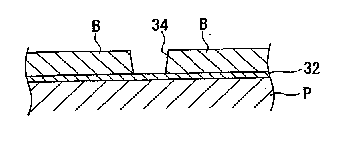
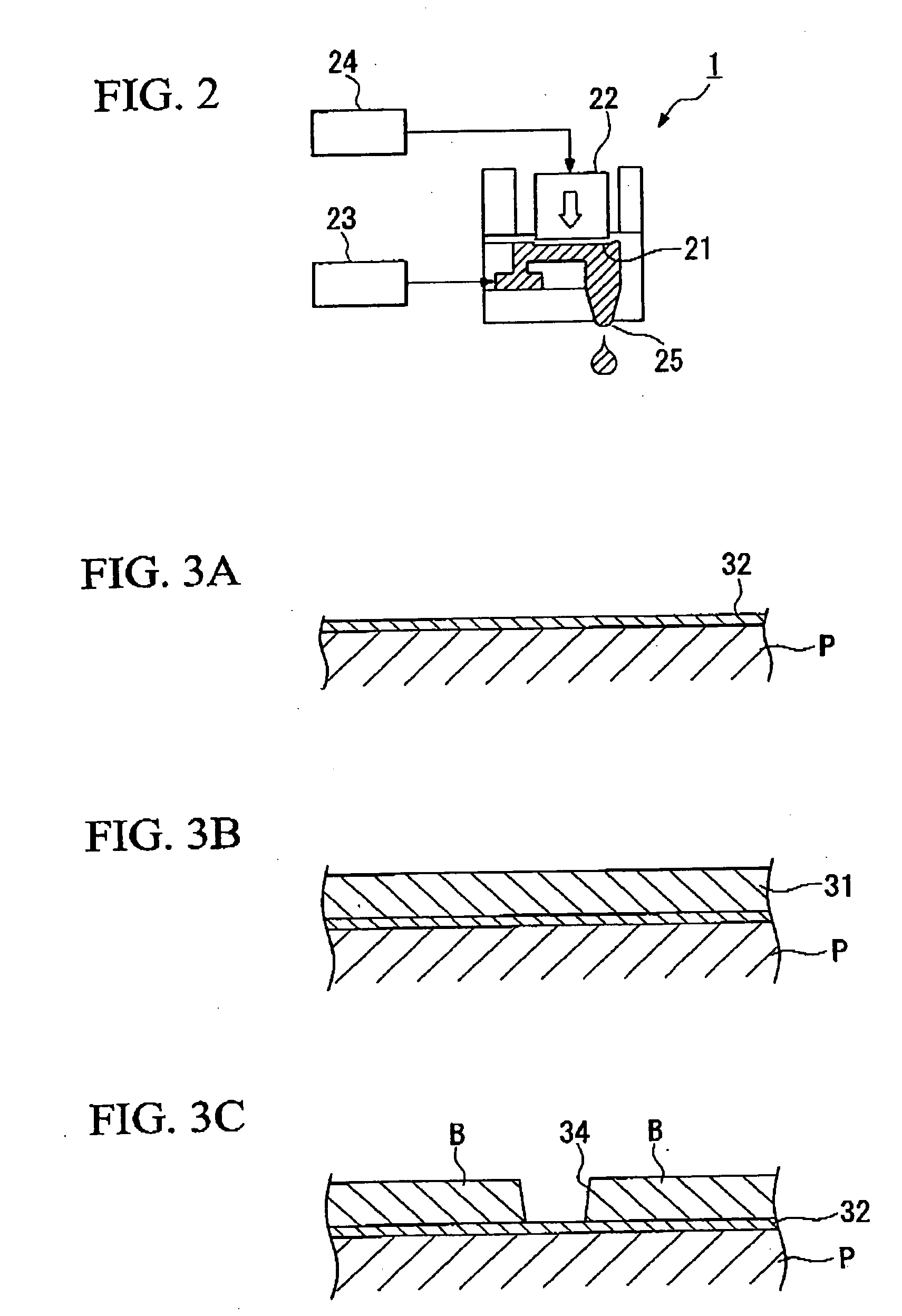
[0067] In this embodiment, a case will be explained, in which a wiring pattern including a plurality of conductive films is formed between banks that are formed depending on the wiring pattern on a substrate, by ejecting ink (function liquid) for a wiring pattern (pattern), which contains conductive fine particles, from an ejecting nozzle of a liquid droplet ejecting head by a liquid droplet ejecting method.

[0068] This ink for a wiring pattern includes dispersion liquid, where conductive fine particles are dispersed in a dispersion medium and a solution where an organic silver compound or silver oxide nano-particles are dispersed in a solvent (dispersion liquid).

[0069] In this embodiment, fine metal particles containing any one of, for example, gold, silver, copper, iron, chrome, manganese, molybdenum, titanium, palladium, tungsten, and nickel, oxides of these, and conductive polymers or fine particles of superconductor, etc. are used as the conductive fine particles.

[0070] It is...

second embodiment

[0136] As a second embodiment, the wiring 33 having a structure which is different from that in the above-mentioned first embodiment will be explained with reference to FIG. 6. In addition, the second embodiment will be explained while focusing on different portions from the above-mentioned first embodiment.

[0137] In this second embodiment, as shown in FIG. 6, ink X3 for a wiring pattern, using titanium as conductive fine particles, and the ink X2 for a wiring patter using silver as conductive fine particles are stacked in the area 34 between the banks by repeatedly performing the material arrangement step and intermediate drying step, which are explained in the above-mentioned first embodiment In addition, as illustrated, the ink X3 for a wiring patter, the ink X2 for a wiring pattern, and the ink X3 for a wiring pattern are stacked in the area 34 between the banks in this order from the substrate P. That is, the ink X2 for a wiring pattern is disposed in the area 34 between the b...

third embodiment

[0141] As a third embodiment, the wiring 33 having a structure which is different from that of the above-mentioned first and second embodiments will be explained with reference to FIG. 7. In addition, the second embodiment will be explained while focusing on different portions from the above-mentioned first embodiment.

[0142] In this third embodiment, as shown in FIG. 7, the ink X1 for a miring pattern, using chromium as conductive fine particles, and the ink X2 for a wiring pattern, using silver as conductive fine particles, are stacked in the area 34 between the banks by repeatedly performing the material arrangement step and intermediate drying step, which are explained in the above-mentioned first embodiment In addition, as illustrated, the ink X1 for a wiring pattern, the ink X2 for a wiring pattern, and the ink X1 for a wiring pattern are stacked in the area 34 between the banks in this order from the substrate P. That is, the ink X2 for a wiring pattern is disposed in the are...


PUM

PropertyMeasurementUnit
Adhesion strengthaaaaaaaaaa
Electrical conductoraaaaaaaaaa
Affinityaaaaaaaaaa

Abstract

A method for fabricating a pattern on a substrate, includes the steps of forming banks according to formation areas of the pattern on the substrate, disposing a first function liquid between the banks, disposing a second function liquid on the function liquid, and applying predetermined treatments to the first and the second function liquids which are disposed between the banks so as to form the pattern with plural materials stacked one on the other.

Description

BACKGROUND OF THE INVENTION [0001] 1. Field of the Invention [0002] The present invention relates to a pattern and to a fabricating method therefor, to a device and to a fabricating method therefor, to an electro-optical apparatus, to an electronic apparatus, and to a method for fabricating an active matrix substrate. [0003] Priority is claimed on Japanese Patent Application No. 2003-133284, filed May 12, 2003, Japanese Patent Application No. 2003-133285, filed May 12, 2003, and Japanese Patent Application No. 2004-118838, filed Apr. 14, 2004, the contents of which are incorporated herein by reference. [0004] 2. Description of the Related Art [0005] Up to now, as a fabricating method for a fie wiring pattern (pattern) of a semiconductor integrated circuit and the like, photolithography methods are frequently used. On the other hand, Japanese Unexamined Patent Application, First Publication No. 11-274671 and Japanese Unexamined Patent Application, First Publication No. 2000-216330 di...

Claims


Application Information

Patent Timeline
IPC IPC(8): B05D5/12B05D7/00G02F1/136G02F1/1343G02F1/1362G09F9/00H01L21/288H01L21/3205H01L21/336H01L21/768H01L21/77H01L27/12H01L27/32H01L29/786H01L51/00H01L51/40H01L51/50H05B33/02H05B33/10H05K3/12
CPCG02F1/136286Y10T428/24802G02F2001/136295H01L21/288H01L21/76838H01L27/12H01L27/3246H01L27/3295H01L29/78669H01L51/0005H01L51/0022H05K3/1241H05K3/125H05K3/1258H05K3/247H05K2203/013H05K2203/0568H05K2203/1173H05K2203/1476H01L27/1292G02F2001/13629H01L21/76885H01L21/76877G02F1/13629G02F1/136295H10K71/135H10K59/122H10K71/611B07C5/3422B07C5/366B07B13/16B03C1/02
Inventor HIRAI, TOSHIMITSU
Owner SEIKO EPSON CORP
Why Eureka
Try Eureka