Addressable microarray device, methods of making, and uses thereof

a microarray and device technology, applied in the field of microarrays, can solve the problems of large amount of time and resources, and the choice of probes is theoretically limited, and achieve the effect of reducing the number of microarrays

Inactive Publication Date: 2005-01-06
3NETICS
View PDF17 Cites 23 Cited by
  • Summary
  • Abstract
  • Description
  • Claims
  • Application Information

AI Technical Summary

Benefits of technology

[0008] One aspect of the present invention relates to a device for performing an array of chemical reactions. The device includes a substrate having a first side, a second side, and an array of microwells. Each microwell within the array includes a porous region defined in the first side and extending partially through the substrate. The porous region is formed by the selective removal of a substrate constituent, such that the porous region is defined by a continuous portion of the substrate. Further, each microwell is capable of holding a sample such that a liquid sample from one microwell does not intermix with a liquid sample from another microwell. Because of the wide range of functional groups, sample molecules, and chemical moieties that can be easily introduced into the described microwells and immobilized therein, particularly onto the porous region of the substrate, the devices of the present invention are useful as supports for the synthesis of compounds, such as biomolecules, and for a range of methods involving chemical reactions and assays.

Problems solved by technology

The procedures utilized often involve large numbers of repetitive steps which consume large amounts of time and resources.
Such probes may be oligonucleotides, proteins, antibodies, or cell-binding molecules and the choice of probes is theoretically limited only by the possibilities of specific binding to or reaction with sample.

Method used


Image

  • Addressable microarray device, methods of making, and uses thereof
  • Addressable microarray device, methods of making, and uses thereof
  • Addressable microarray device, methods of making, and uses thereof

Examples


example 1

Production of a Substrate having an Array of Microwells

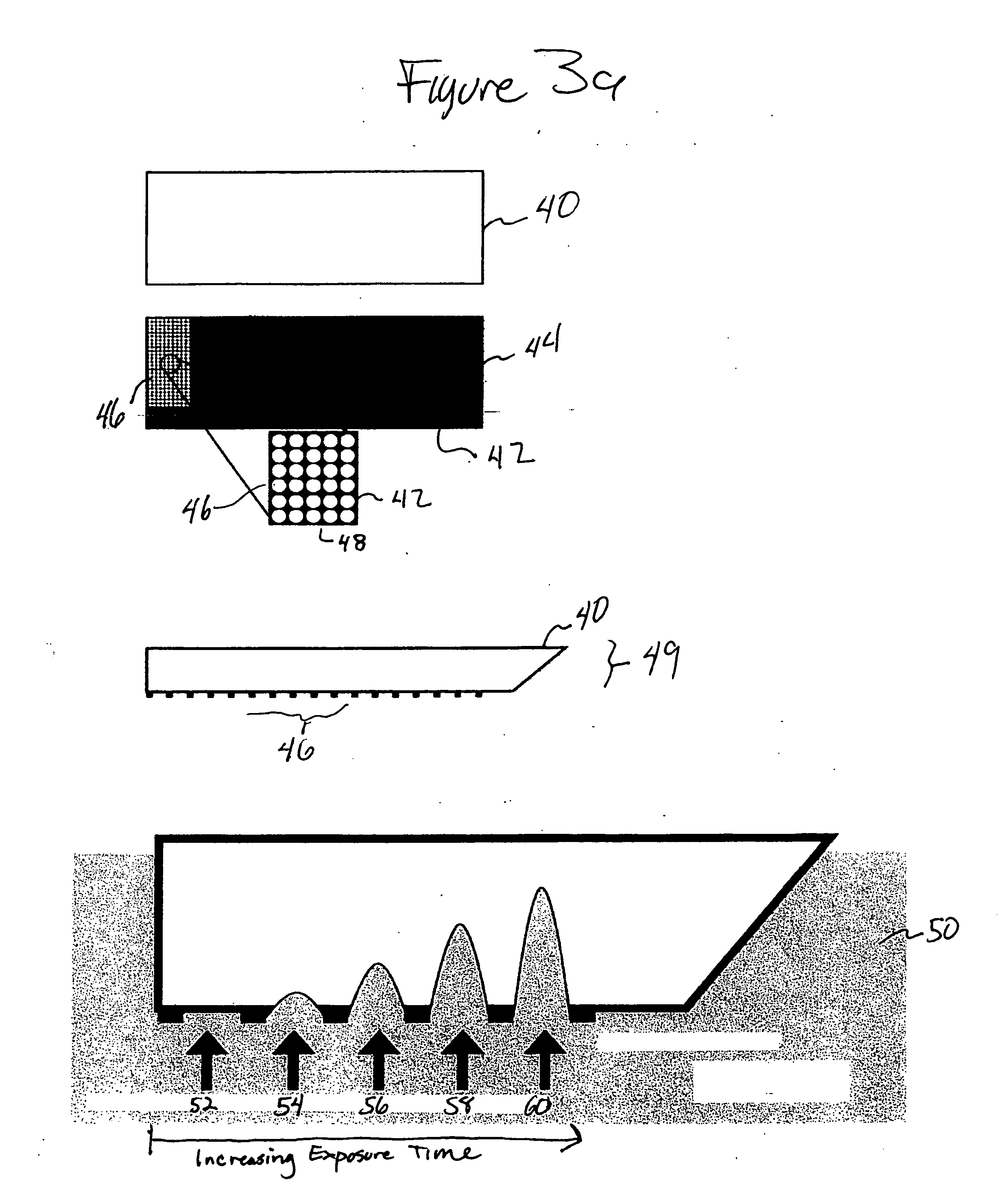
[0101]FIGS. 3a and 3b illustrate one method of producing a substrate having an array of microwells according to an embodiment of the invention. In the first step, a suitable substrate 40 is provided. Second, a mask is applied to the a side of the substrate. A mask 42 is applied to a second side 44 of the substrate 40. The mask 42 contains a plurality of openings 46, further illustrated in a expanded window 48, which selectively allows exposure of the second side 44 of the substrate 40 to an etchant. A side view 49 of the substrate illustrating the openings of the mask is shown. Next, the substrate 40 is at least partially immersed in an etching bath. The etchant contacts the substrate areas not covered by the mask, thereby removing substrate material and forming cavities at openings 52, 54, 56, 58, 60 in selected areas. FIG. 3a shows exposure for increasing amounts of time and illustrates that the degree to which the substrate ...


PUM

PropertyMeasurementUnit
sizeaaaaaaaaaa
sizeaaaaaaaaaa
sizeaaaaaaaaaa

Abstract

The present invention relates to devices and methods for performing an array of chemical reactions. The device includes a substrate having an array of microwells. Each microwell within the array includes a porous region defined in the first side and extending partially through the substrate. The porous region is formed by the selective removal of a substrate constituent, such that the porous region is defined by a continuous portion of the substrate. A wide range of functional groups, sample molecules, and chemical moieties that can be easily introduced into the described microwells and immobilized therein, particularly onto the porous region of the substrate, therefore the devices of the present invention are useful as supports for the synthesis of compounds, such as biomolecules, and for a range of methods involving chemical reactions and assays.

Description

CROSS REFERENCE TO RELATED APPLICATION [0001] This application claims priority under 35 U.S.C. § 119(e)(1) to U.S. Provisional Application Ser. No. 60 / 453,932, filed Mar. 11, 2003, herein incorporated by reference in its entirety.BACKGROUND OF THE INVENTION [0002] 1. Field of the Invention [0003] The invention relates generally to microarrays for synthesizing and analyzing molecules, and more specifically to methods and devices having an array of microwells suitable for performing a plurality of chemical reactions, assays, and synthesis reaction. [0004] 2. Background Information [0005] Chemical analysis, detection and synthesis of biomolecules has become very important in research and in many industries, and the analysis of biological molecules such as nucleic acids and proteins forms the basis of various assays. The procedures utilized often involve large numbers of repetitive steps which consume large amounts of time and resources. (see, e.g., Sambrook, J., et al., Molecular Cloni...

Claims


Application Information

Patent Timeline
Patent Type & Authority Applications(United States)
IPC IPC(8): B01J19/00B01L3/00C12M1/34C12Q1/68C40B40/06C40B40/10C40B40/18C40B60/14
CPCB01J19/0046B01L2300/0896B01J2219/00317B01J2219/00432B01J2219/00497B01J2219/00574B01J2219/00576B01J2219/00585B01J2219/00596B01J2219/00605B01J2219/00621B01J2219/00644B01J2219/00653B01J2219/00659B01J2219/00689B01J2219/00711B01J2219/00722B01J2219/00725B01J2219/00738B01J2219/00745B01J2219/0075B01L3/5025B01L2300/069B01L2300/0819B01L2400/0415B82Y30/00C40B40/06C40B40/10C40B40/18C40B60/14B01L3/5085B01L2200/12B01L2300/0893B01J2219/00286
Inventor O'CONNOR, DAVIDNORTON, BARTONKLEIN, GERALD
Owner 3NETICS
Why Eureka
Try Eureka