Semiconductor device, electronic device, electronic apparatus, and method of manufacturing semiconductor device
- Summary
- Abstract
- Description
- Claims
- Application Information
AI Technical Summary
Benefits of technology
Problems solved by technology
Method used
Image

Examples
first embodiment
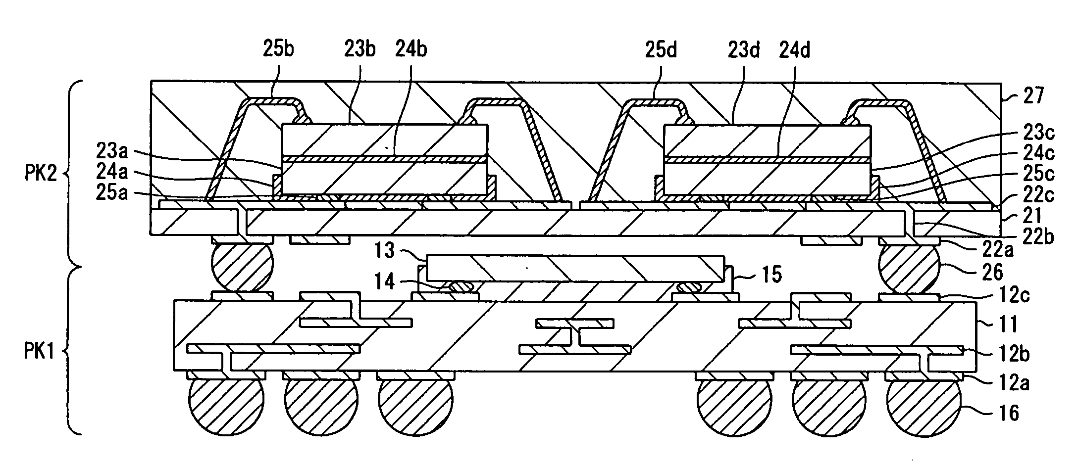
[0031] Hereinafter, semiconductor devices according to embodiments of the present invention will be described by referring to the drawings. FIG. 1 is a sectional view showing a schematic structure of a semiconductor device according to the present invention.
[0032] In FIG. 1, a semiconductor package PK1 has a carrier substrate 11 provided therein, lands 12a and 12c are formed on both sides of the carrier substrate 11, and internal wiring 12b is formed inside the carrier substrate 11. Then, a semiconductor chip 13 is flip-chip mounted above the carrier substrate 11, and a protruding electrode 14 for flip-chip mounting is formed on the semiconductor chip 13. Then, the protruding electrode 14, formed on the semiconductor chip 13, is bonded to the land 12c by Anisotropic Conductive Film (ACF) bonding via an anisotropic conductive film 15. Moreover, on the land 12a formed on the back surface of the carrier substrate 11, a protruding electrode 16 for mounting the carrier substrate 11 above...
second embodiment
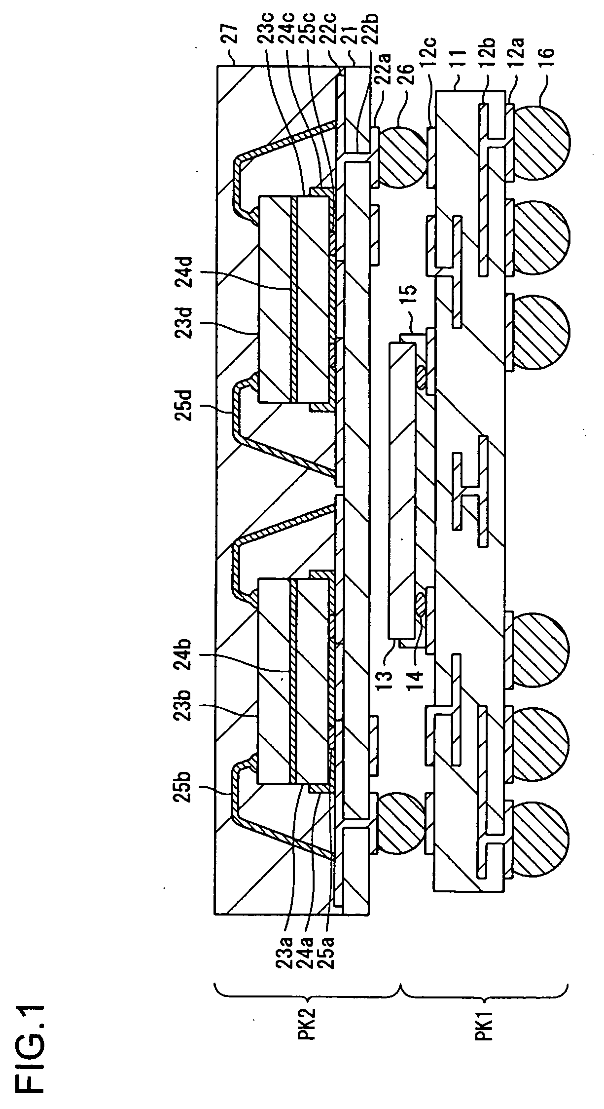
[0041] Moreover, in the above described embodiment, as for the semiconductor package PK1, a flip-chip mounted structure has been described as an example. However, a molded structure may be used. Moreover, the semiconductor package PK2 may be of a single layer structure of a semiconductor chip as well as a stacked structure of semiconductor chips, and may be of a flip-chip structure as well as a molded structure. FIG. 2 is a sectional view showing a schematic structure of a semiconductor device according to the present invention.
[0042] In FIG. 2, a semiconductor package PK11 has a carrier substrate 31 provided therein, lands 32a and 32c are formed on both sides of the carrier substrate 31, and an internal wiring 32b is formed in the carrier substrate 31. Then, a semiconductor chip 33 is flip-chip mounted on the carrier substrate 31, and a protruding electrode 34 for flip-chip mounting is formed on the semiconductor chip 33. Then, the protruding electrode 34, formed on the semiconduct...
third embodiment
[0049]FIG. 3 is a plan view showing a method of arranging protruding electrodes according to the present invention. In FIG. 3, on carrier substrates 62 and 64, protruding electrodes 63 and 65 are arranged in a U-shape, respectively, and regions, where the protruding electrodes 63 and 65 are not arranged, are provided along at least one side of the carrier substrates 62 and 64.
[0050] Then, the protruding electrodes 63 and 65, formed on the carrier substrates 62 and 64 respectively, are bonded to a lower substrate, above which the semiconductor chip 61 is provided, so that the regions, where the protruding electrodes 63 and 65 are not formed, overlap above the semiconductor chip 61. Accordingly, even when the carrier substrates 62 and 64 are mounted so that the ends of the carrier substrates 62 and 64 are arranged above the semiconductor chip 61, the stability of the carrier substrates 62 and 64 can be maintained, and while suppressing complication of the manufacturing process, a spac...
PUM
 Abstract
Description
Claims
Application Information
 - R&D
- Intellectual Property
- Life Sciences
- Materials
- Tech Scout
- Unparalleled Data Quality
- Higher Quality Content
- 60% Fewer Hallucinations
Browse by: Latest US Patents, China's latest patents, Technical Efficacy Thesaurus, Application Domain, Technology Topic, Popular Technical Reports.
© 2025 PatSnap. All rights reserved.Legal|Privacy policy|Modern Slavery Act Transparency Statement|Sitemap|About US| Contact US: help@patsnap.com