Detector for alpha particle or cosmic ray
- Summary
- Abstract
- Description
- Claims
- Application Information
AI Technical Summary
Benefits of technology
Problems solved by technology
Method used
Image
Examples
first embodiment
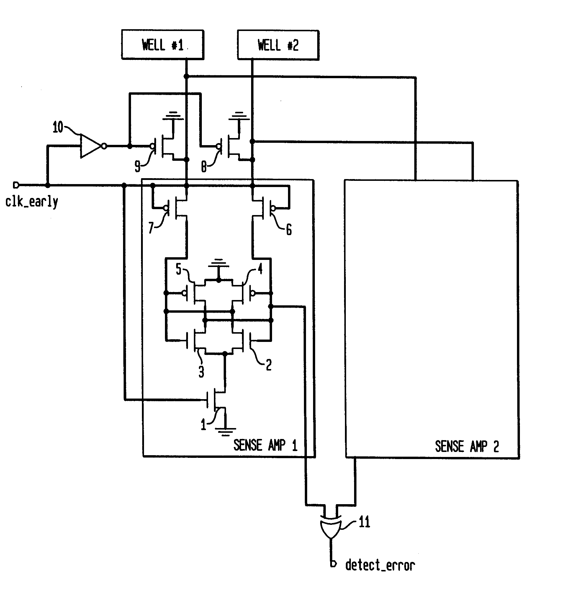
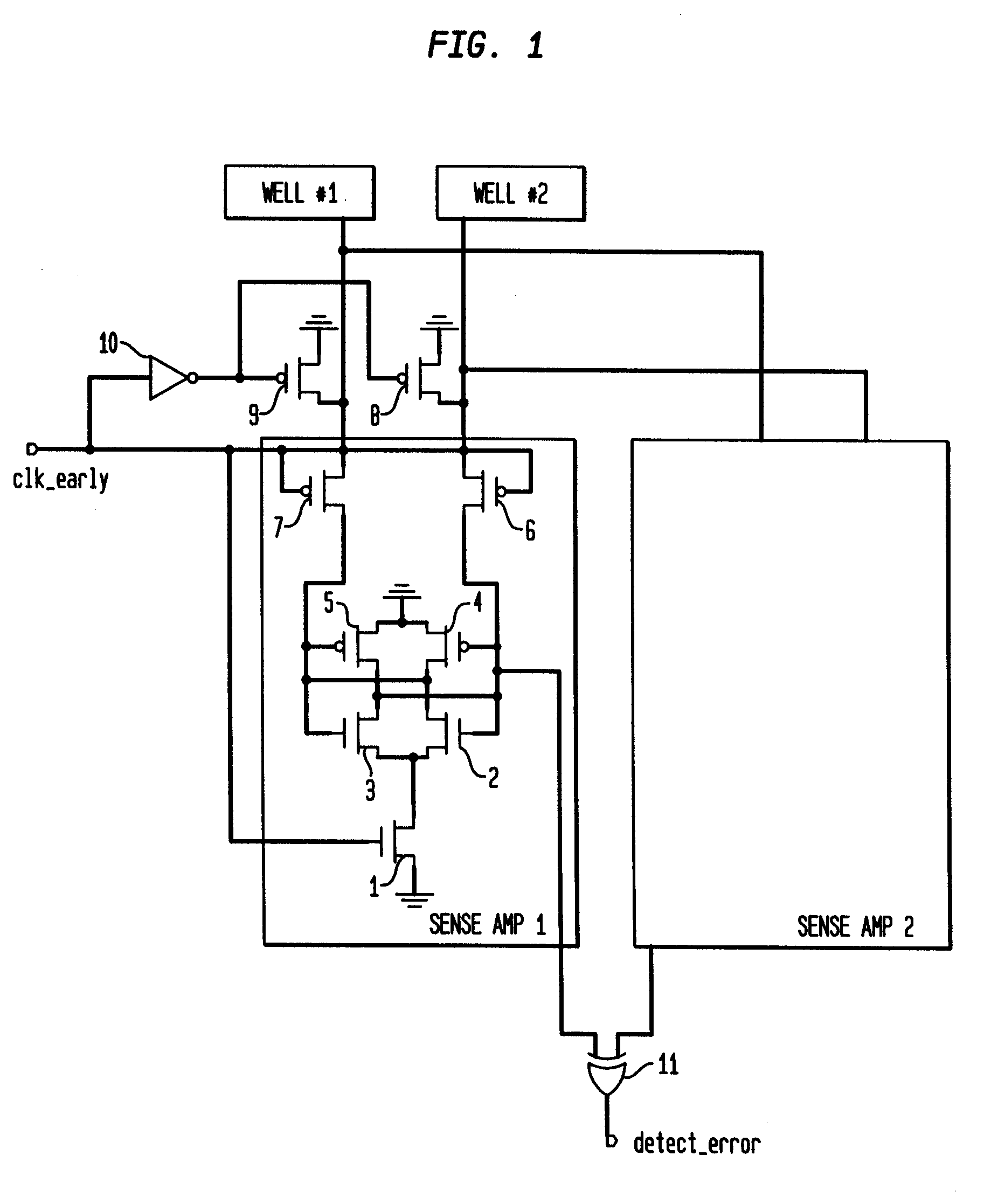
[0015]FIG. 1 illustrates a detector circuit pursuant to the present invention for detecting an SER event (alpha particle or cosmic ray strike) of a first silicon P well 1 or a second silicon P well 2, by differentially detecting the floating voltages of the first and second silicon wells during periods of non-operation of the circuits fabricated in the first and second silicon wells. Each of the silicon P wells 1 and 2 is connected to two Sense Amps (SA) 1 and 2 which are substantially identical, with FIG. 1 only illustrating the circuit details of Sense Amp 1. A single Sense Amp is able to detect that one of the two wells 1 and 2 incurred an SER event, but would not be able to detect which one of the two wells 1 and 2 incurred the SER event. Two Sense Amps 1 and 2 are provided to be able to detect which one of the two wells 1 and 2 incurred the SER event, as explained below.
[0016] The silicon wells 1 and 2 are connected to their bias power supplies through respective feeder devices...
second embodiment
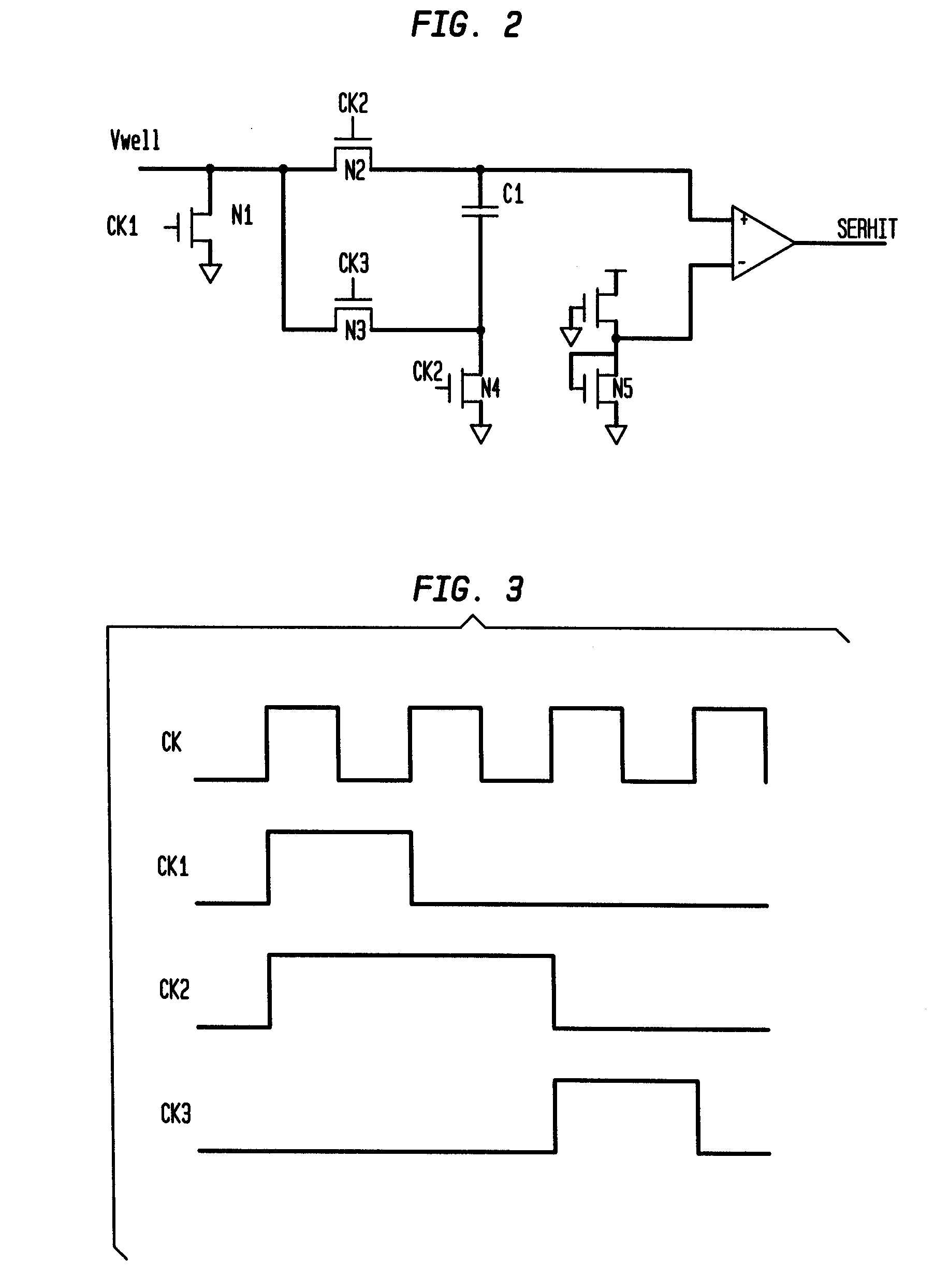
[0027]FIG. 2 illustrates the present invention in which a detector circuit monitors a single silicon well in a silicon substrate for an SER event by monitoring the background voltage level of the single silicon well over a period of time. In this embodiment, the silicon well voltage Vwell during a first sampling period of time is compared with the silicon well voltage Vwell over a second sampling period of time to detect a deviation in the silicon well voltage which is indicative of an SER event. The circuit of FIG. 2 is a capacitive sensing detector circuit which takes a correlated double sampling of the background voltage level of the Vwell node voltage to allow offset cancellation of base leakage current and noise current injection of the Vwell node.
[0028]FIG. 3 illustrates timing diagrams for the clock control signals for the circuit of FIG. 2. In the circuit of FIG. 2 the sampled well node voltage Vwell is input to a first device N1 coupled between Vwell and ground and controll...
PUM
 Abstract
Description
Claims
Application Information


