

Display device
- Summary
- Abstract
- Description
- Claims
- Application Information
AI Technical Summary
Benefits of technology
Problems solved by technology
Method used
Image

Examples
embodiment mode 1
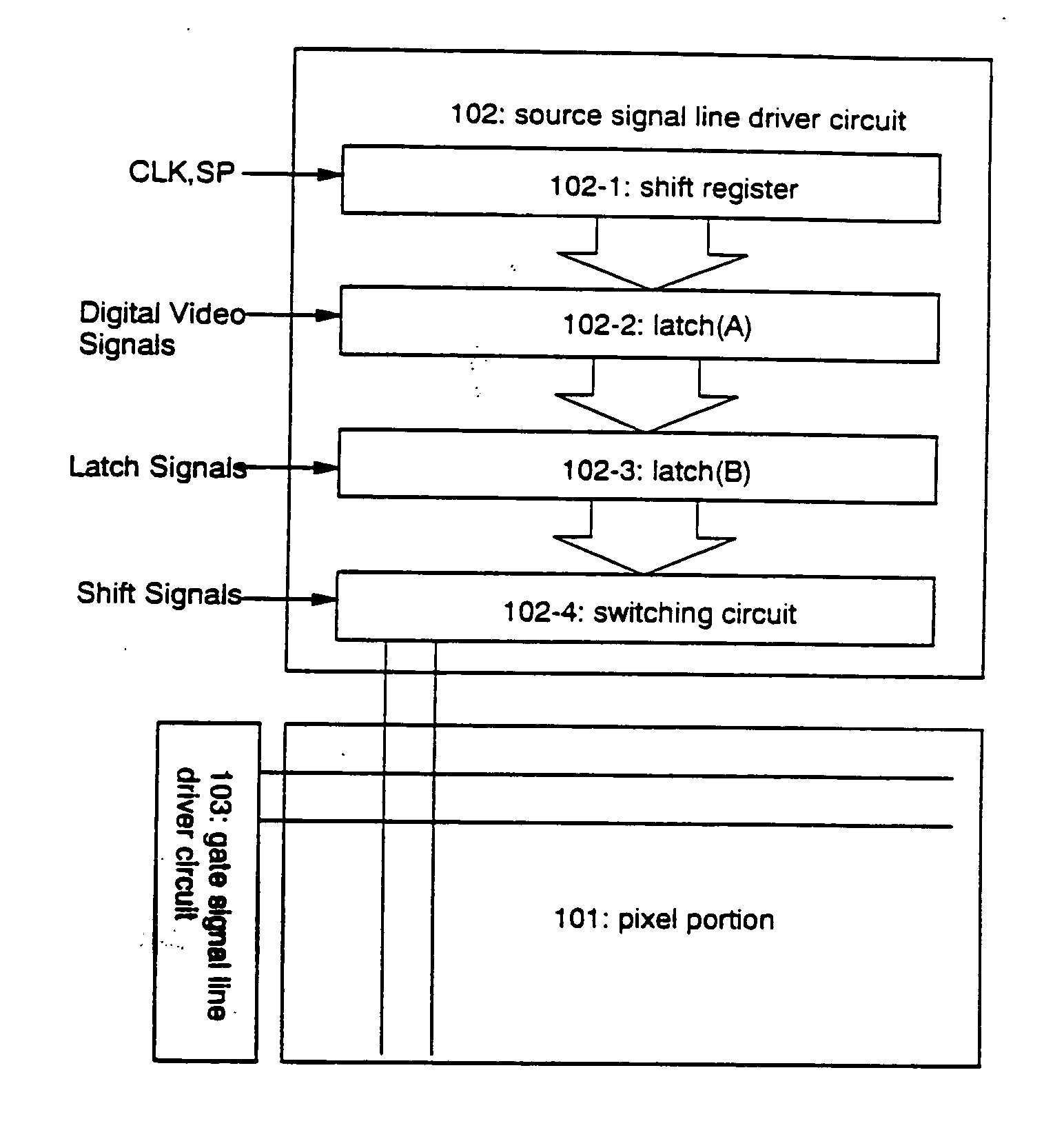
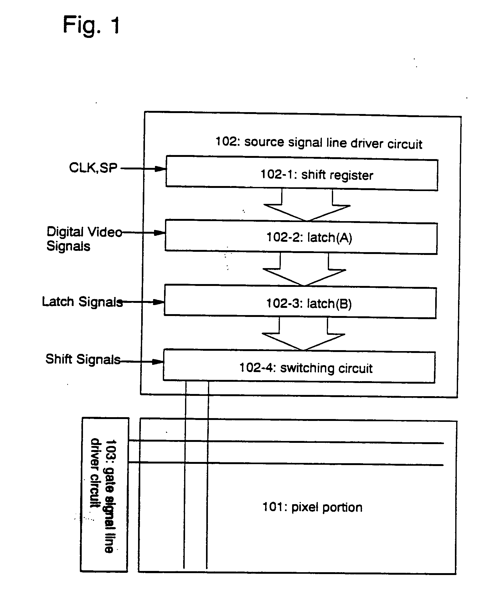
[0077] A first structure in accordance with the present invention will be now described. FIG. 1 shows a block diagram of a light emitting device having the first structure in accordance with the present invention.
[0078] Reference numeral 101 denotes a pixel portion in which a plurality of pixels are provided in matrix. Reference numerals 102 and 103 denote a source signal line driver circuit and a gate signal line driver circuit, respectively.
[0079] The source signal line driver circuit 102 includes a shift register 102-1, a latch (A) 102-2, a latch (B) 102-3, and a switching circuit 102-4. It should be noted that the source signal line driver circuit of the present invention may further include a level shift, a buffer or the like, in addition to the components mentioned above.
[0080] Although not illustrated, the gate signal line driver circuit 103 includes a shift register and a buffer. In some cases, the gate signal line driver circuit 103 may further include a level shift in a...
embodiment mode 2
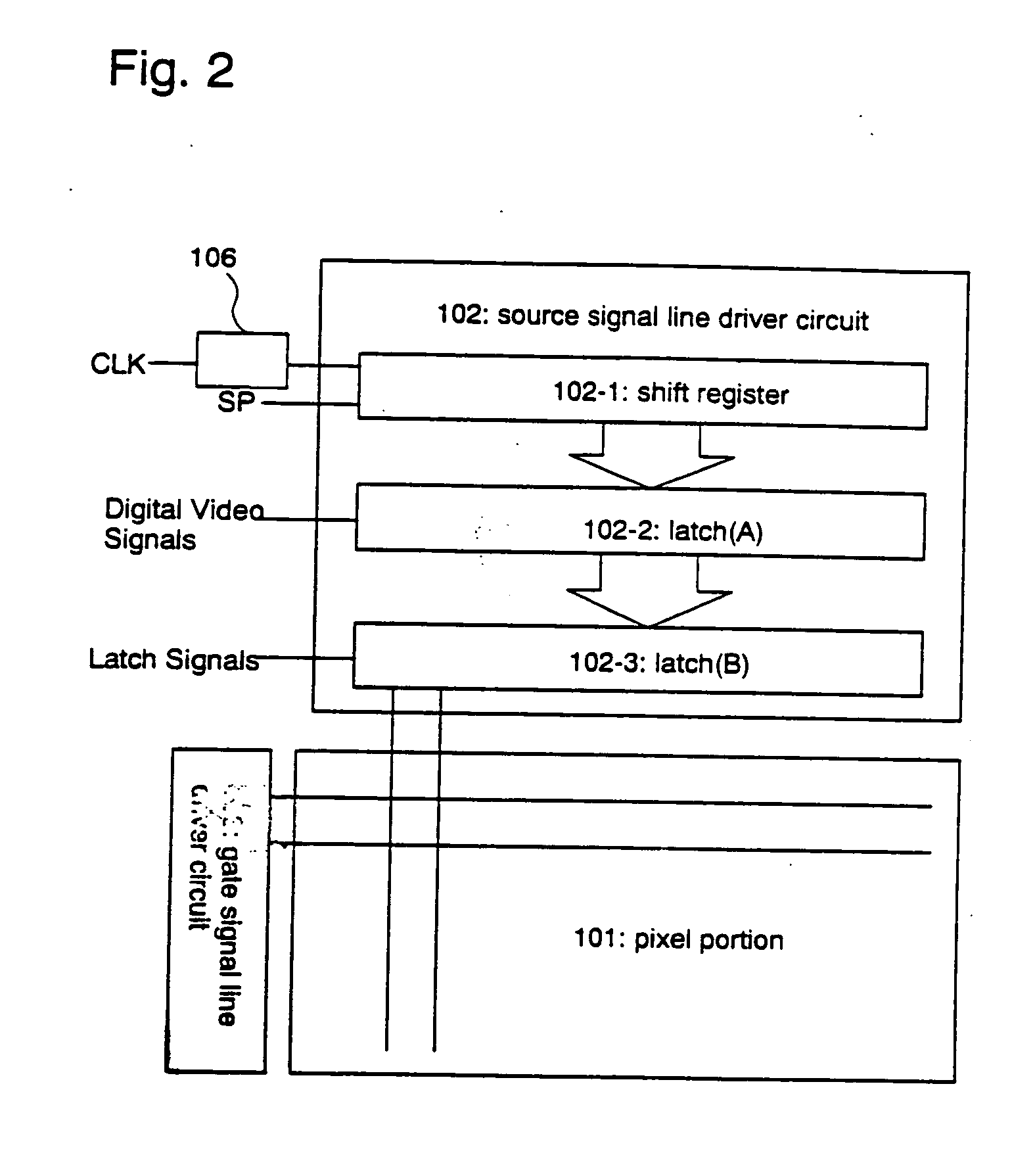
[0100] A second structure in accordance with the present invention will be now described. FIG. 2 shows a block diagram of a light emitting device having the second structure in accordance with the present invention. In FIG. 2, the same components as shown in FIG. 1 are designated with the same reference numerals.
[0101] The light emitting device in the present embodiment mode employs a clock signal control circuit 106 which allows a constant electrical potential instead of the clock signal (CLK) to be applied to the shift register 102-1.
[0102] More specifically, the light emitting device is configured to input a constant electrical potential (fixed electrical potential) into the shift register 102-1, instead of the clock signal, for a constant time period by means of the clock signal control circuit 106. The above structure prevents the timing signal that is to be used for inputting the digital video signal at less significant bits in the range from the first bit to the m-th bit (m...
embodiment mode 3
[0107] Another example of the second structure in accordance with the present invention, which is different from the one described in Embodiment Mode 2, will be now described. FIG. 3 shows a block diagram of a light emitting device having the second structure in accordance with the present invention. In FIG. 3, the same components as shown in FIG. 1 are designated with the same reference numerals.
[0108] The light emitting device in the present embodiment mode employs a timing signal control circuit 107 which allows a constant electrical potential, instead of the timing signal output from the shift register 102-1, to be applied to the latch (A) 102-2.
[0109] More specifically, the light emitting device is configured to input a constant electrical potential (fixed electrical potential) into the latch (A) 102-2, instead of the timing signal output from the shift register 102-1, for a constant time period by means of the timing signal control circuit 107. The above structure prevents t...
PUM
 Abstract
Description
Claims
Application Information