Spread-spectrum clock signal generator

a clock signal and spread-spectrum technology, applied in the direction of pulse automatic control, angle modulation details, demodulation, etc., can solve the problems of reducing as far as possible the level of electromagnetic emissions, undetectable electromagnetic emissions of electronic equipment and appliances, and even harmful to the human body, so as to achieve low electromagnetic emissions

Inactive Publication Date: 2005-01-20
ACCENT INC
View PDF8 Cites 28 Cited by
  • Summary
  • Abstract
  • Description
  • Claims
  • Application Information

AI Technical Summary

Benefits of technology

In view of the state of the art outlined above, it has been an object of the present invention to provide a clock signal generator having low electromagnetic emissions.

Problems solved by technology

Electromagnetic emissions by electronic equipments and appliances are highly undesired, because they are a cause of disturb (interference) of the operation of other electronic equipments.
In some cases, electromagnetic emissions are even harmful to the human body.
Reducing as far as possible the level of electromagnetic emissions is therefore a major issue that electronic circuit designers have to cope with.
The main drawbacks of these techniques are bulkiness, relatively high cost, and scarce flexibility.
The Applicant has observed that a problem with this technique is that it does not enable to carefully control the modulation amount; the VCO gain is in fact hardly predictable, especially in integrated circuits, because it depends on several parameters such as the temperature.
Also in this case, the modulation index is poorly controlled.
The Applicant has observed that in the prior-art spread-spectrum clock generators that relies on a PLL, with a modulation signal directly driving the VCO, the modulation index cannot be tightly controlled, because the loop, due to the relatively narrow bandwidth, does not work in locked condition; the continuous variation of the clock frequency causes the PLL to be always in a capture transient.

Method used


Image

  • Spread-spectrum clock signal generator
  • Spread-spectrum clock signal generator
  • Spread-spectrum clock signal generator

Examples


Embodiment Construction

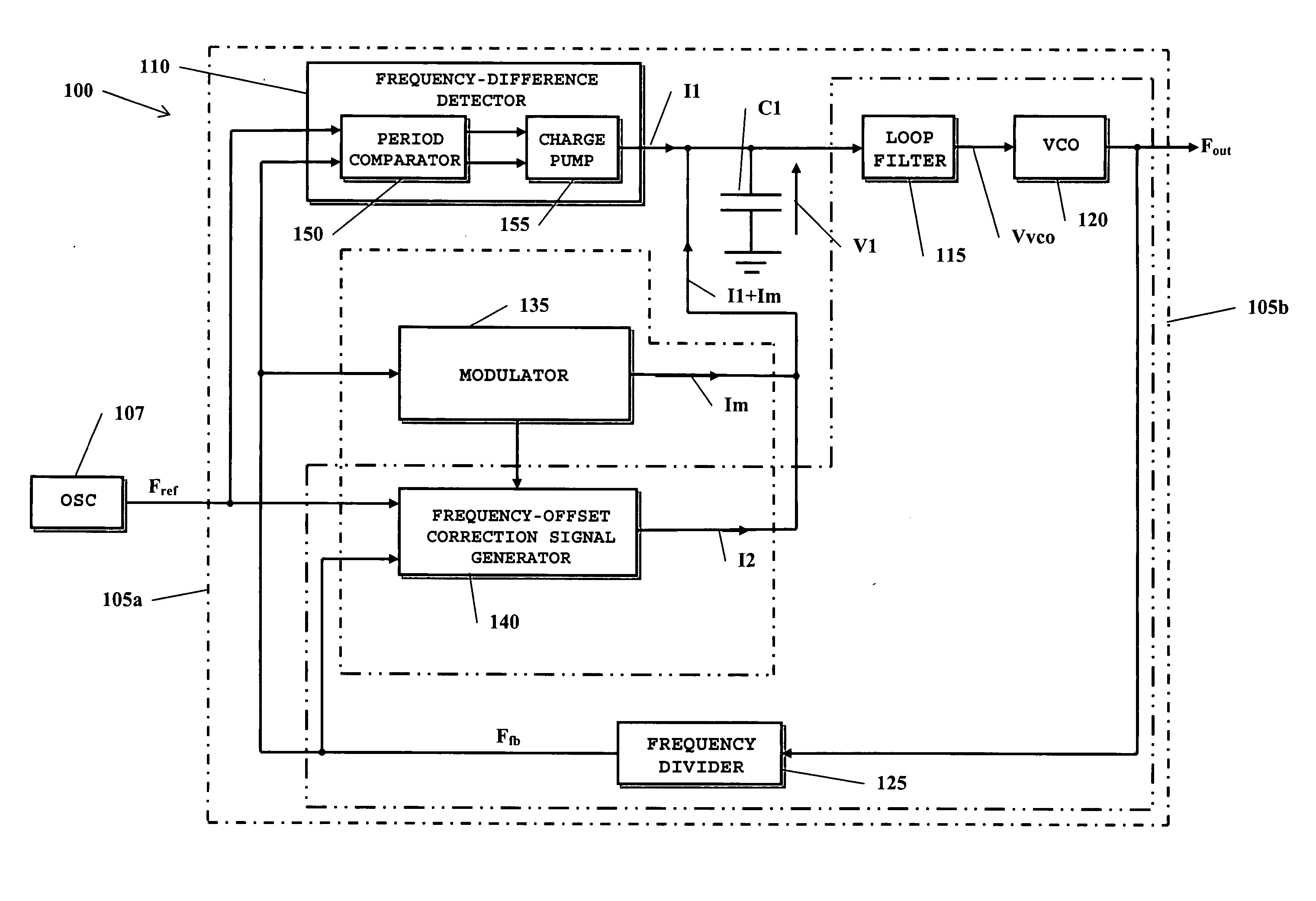
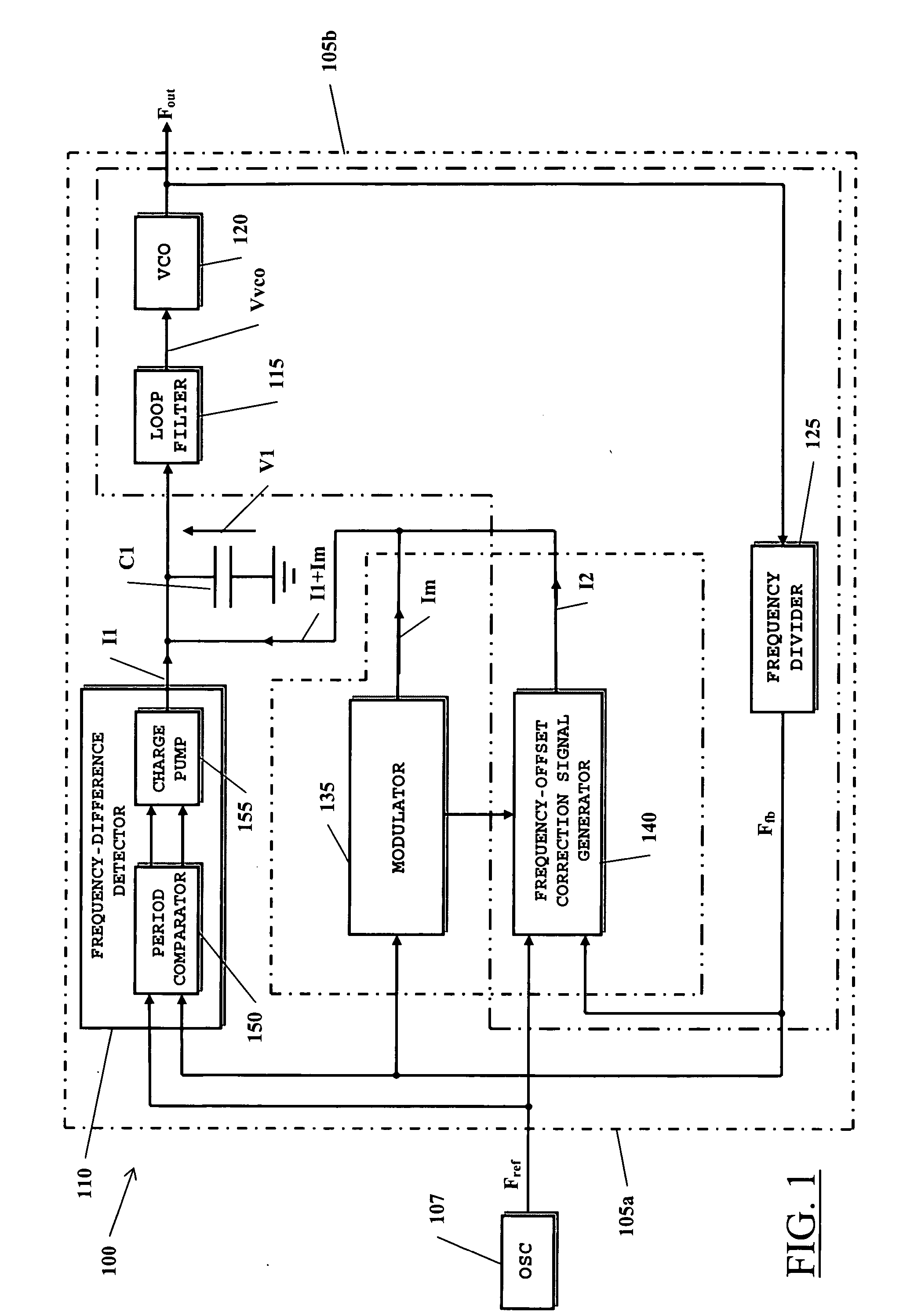
With reference to the drawings, FIG. 1 schematically shows a spread-spectrum clock signal generator according to an embodiment of the present invention, globally indicated as 100.

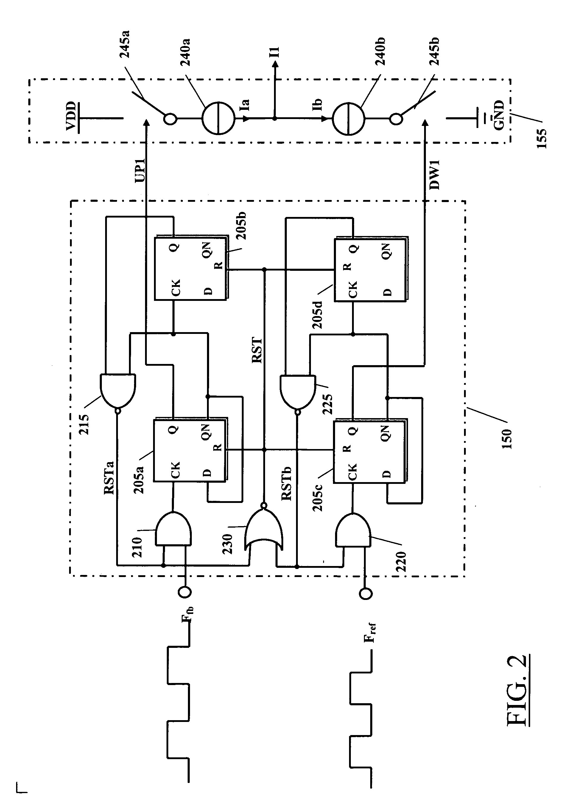
The clock signal generator 100 comprises a first circuit loop 105a, in the drawing circumscribed by dash-and-dot lines. The first circuit loop 105a includes a frequency-difference detector 110 that receives a reference signal Fref, oscillating at a prescribed frequency Fref (in the following, the reference frequency), and a feedback signal Ffb. The reference signal Fref is for example generated by a local oscillator 107, e.g. a crystal oscillator. The frequency-difference detector 110 is sensitive to the frequency difference between the reference signal Fref and the feedback signal Ffb, and generates a signal I1, particularly a current signal, which, on average, has a value proportional to the frequency difference between the reference signal Fref and the feedback signal Ffb. A frequency-difference detec...


PUM


Abstract

A spread-spectrum clock signal generator comprises a circuit loop receiving a reference signal at a reference frequency and adapted to generate an output signal at an output frequency dependent on and locked to the reference frequency, and a modulator circuit generating a modulation signal at a modulation frequency; the modulation signal is injected into the circuit loop to induce a modulation of the frequency of the output signal with respect to the frequency dependent on the reference frequency. The circuit loop is a frequency-locked loop and has a bandwidth sufficiently higher than the modulation frequency, so that the output frequency tracks the modulation signal. Frequency-offset correction means are further provided, for evaluating a frequency offset between an average frequency of the output signal and the frequency dependent on the reference frequency, and for generating a frequency-offset correction signal which is injected into the circuit loop for correcting the evaluated frequency offset.

Description

PRIORITY CLAIM This application claims priority from European patent application No. 03425257.7, filed Apr. 28, 2003, which is incorporated herein by reference. FIELD OF THE INVENTION The present invention generally relates to methods and systems for reducing electromagnetic emissions by electronic circuits, and particularly to methods and systems based on the so-called Spread-Spectrum Technology (shortly, SST). Even more particularly, the invention concerns a spread-spectrum clock signal generator. BACKGROUND OF THE INVENTION Electromagnetic emissions by electronic equipments and appliances are highly undesired, because they are a cause of disturb (interference) of the operation of other electronic equipments. In some cases, electromagnetic emissions are even harmful to the human body. Many national and international regulatory authorities have therefore issued prescriptions (generally referred to as ElectroMagnetic Interference or, shortly, EMI regulations) aiming at setting m...

Claims


Application Information

Patent Timeline
Patent Type & Authority Applications(United States)
IPC IPC(8): H03L7/087H03L7/089H03L7/095H04B15/02
CPCH03L7/087H03L7/0891H04B2215/067H04B15/02H03L7/095
Inventor GIUNCO, FABIOGARDELLINI, DANIELEBALLERINI, MASSIMO
Owner ACCENT INC
Why Eureka
Try Eureka