

Fabrication of silicon-on-nothing (SON) MOSFET fabrication using selective etching of Si1-xGex layer
a technology of mosfet and fabrication method, which is applied in the direction of semiconductor devices, electrical equipment, transistors, etc., can solve the problems of higher parasitic source and drain capacitance, and the requirement for exceptionally thin silicon and buried oxide films exceeds the present manufacturing capability of soi wafers
- Summary
- Abstract
- Description
- Claims
- Application Information
AI Technical Summary
Problems solved by technology
Method used
Image

Examples
Embodiment Construction
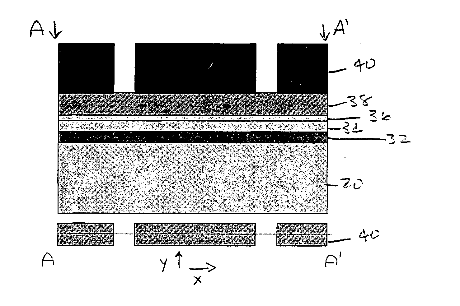
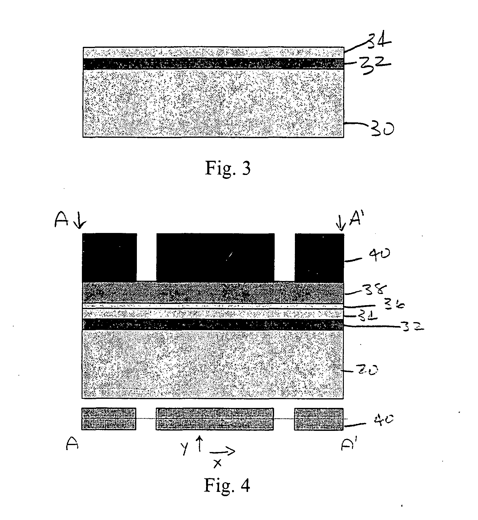
[0015] In the method of the invention, an epitaxial Si1-xGex layer is formed on a silicon substrate. A thin silicon layer, e.g., less than 100 nm, is epitaxially deposited on the Si1-xGex on the silicon substrate. Because of the lattice mismatch between the silicon and Si1-xGex the thickness of Si1-xGex has to be less than the critical thickness of Si1-xGex so that no relaxation occurs and no defects form. After trench etching of the top silicon and Si1-xGex into the silicon substrate to form a first trench, the Si1-xGex layer is selectively removed by etching. The etching time is controlled so that some SiGe remains on the smallest features of the structure to prevent lifting of the silicon. A layer of SiO2 is then deposited by CVD to fill the first trench. A second trench etch step and selective etching of the Si1, Ge, layer follows. The SiO2 layer deposited by CVD after the first selective Si1-xGex etch anchors the silicon island in place during the second selective Si1-xGex etch...
PUM
| Property | Measurement | Unit |
|---|---|---|
| critical thickness | aaaaa | aaaaa |
| critical thickness | aaaaa | aaaaa |
| thickness | aaaaa | aaaaa |
Abstract
Description
Claims
Application Information