Intermediate substrate, intermediate substrate with semiconductor element, substrate with intermediate substrate, and structure having semiconductor element, intermediate substrate and substrate

a technology of intermediate substrates and substrates, which is applied in the direction of printed circuit non-printed electric components association, sustainable manufacturing/processing, and final product manufacturing, etc., can solve the problems of reducing the stability of the ic chip. , to achieve the effect of avoiding the complexity of the structure and the increase in the step number of the intermediate substrate, and reducing the cost of the entire structur

Inactive Publication Date: 2005-02-03
NGK SPARK PLUG CO LTD
View PDF7 Cites 69 Cited by
  • Summary
  • Abstract
  • Description
  • Claims
  • Application Information

AI Technical Summary

Benefits of technology

[0081] The ceramics to be selected as the material to make the intermediate substrate body may have the insulating properties, as described above. This is because the intermediate substrate body having no insulating properties has to be provided beforehand with the insulating layer when the conductor structure such as the conductor columns is to be formed, but the intermediate substrate body having the insulating properties does not require that insulating layer. As a result, it is possible to avoid the complexity of the structure and the increase in the step number of the intermediate substrate

Problems solved by technology

When the high thermal stress acts on the interface or the like between the IC chip and the intermediate substrate, moreover, a crack or the like may occur in the IC chip mounting portion (or the joint portion).
Therefore, there arises a problem that a high connection reliability cannot be given between the IC chip and the intermediate substrate.
Especially if any of the sides of the IC chip exceeds 10.0 mm, an especially high thermal stress may act to cause the crack or the like.
If the IC chip has a thickness smaller than 1.0 mm, on the other hand, the strength may be weakened to cau

Method used


Image

  • Intermediate substrate, intermediate substrate with semiconductor element, substrate with intermediate substrate, and structure having semiconductor element, intermediate substrate and substrate
  • Intermediate substrate, intermediate substrate with semiconductor element, substrate with intermediate substrate, and structure having semiconductor element, intermediate substrate and substrate
  • Intermediate substrate, intermediate substrate with semiconductor element, substrate with intermediate substrate, and structure having semiconductor element, intermediate substrate and substrate

Examples


Embodiment Construction

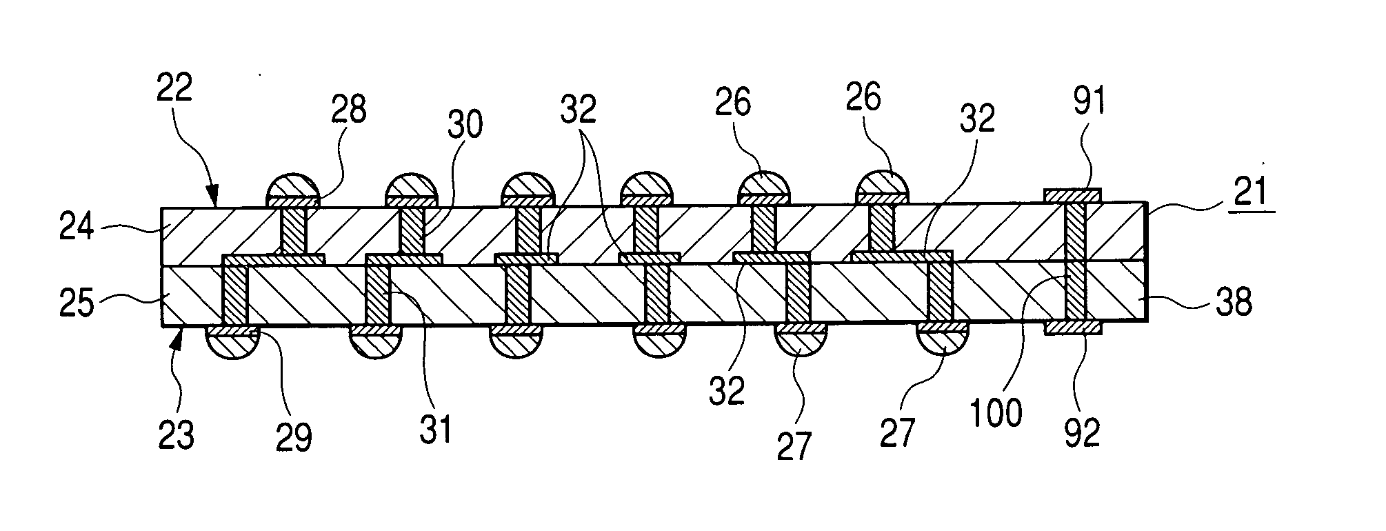
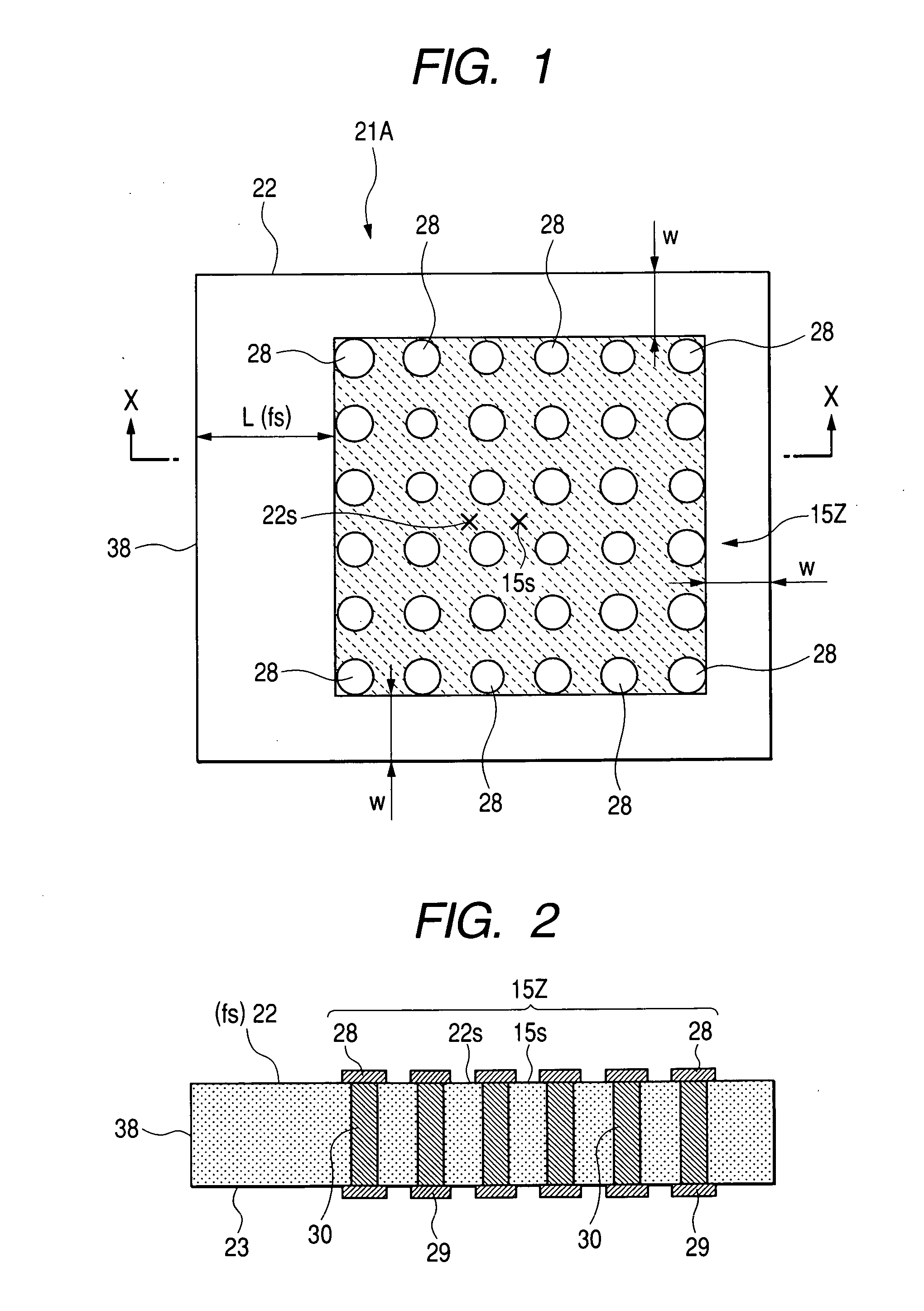
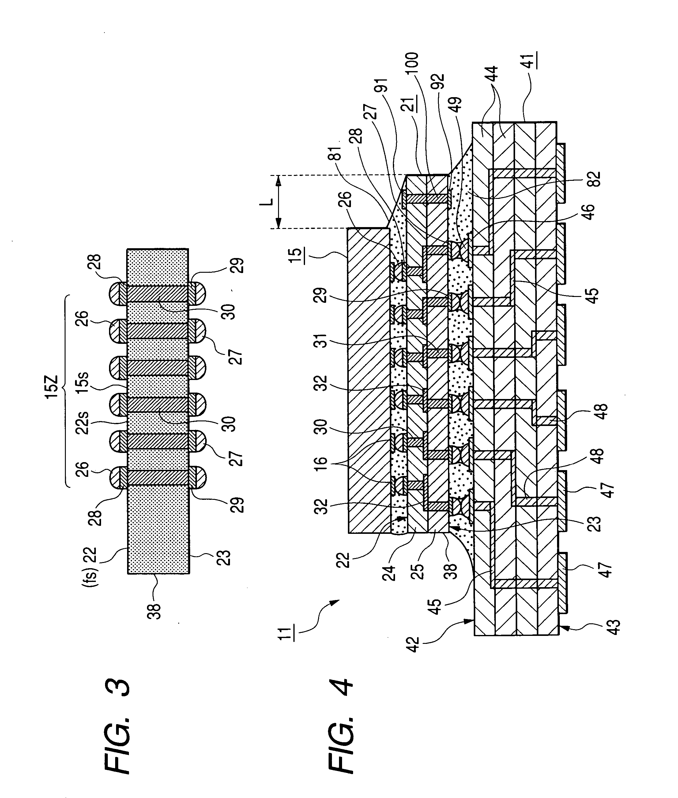
[0112] One embodiment of the invention will be described in detail with reference to FIG. 1 and so on. FIG. 1 is a top plan view of an interposer (or an intermediate substrate) 21A; FIG. 2 is a sectional view taken along line X-X of FIG. 1; and FIG. 3 is a schematic view showing the state, in which solder bumps 26 and 27 are formed over first and second face terminals 28 and 29. FIG. 4 is a schematic section showing a semiconductor package structure (as will also be called the “structure”) of this embodiment, which is composed of an IC chip (or a semiconductor element) 15, an interposer 21 (or an intermediate substrate) 21, and a wiring substrate (as will also be called the “substrate”) 41 as an IC package substrate. FIG. 5 is a schematic section showing the interposer 21, and FIG. 6 is an enlarged top plan view showing a portion of the interposer 21. FIG. 7 is a schematic section showing an interposer 61 with the IC chip (or the intermediate substrate with the semiconductor element...


PUM


Abstract

An intermediate substrate comprising: an intermediate substrate body containing an insulating material, and having a first face to be mounted with an semiconductor element and a second face opposing to said first face; and a semiconductor element mounting area including a plurality of first face terminals arranged on said first face, and being surrounded by an outermost periphery of said plurality of first face terminals, wherein a center of said semiconductor element mounting area is eccentric with respect to a center of said first face.

Description

FIELD OF THE INVENTION [0001] The present invention relates to an intermediate substrate, an intermediate substrate with a semiconductor element, a substrate with an intermediate substrate, and a structure having a semiconductor element, an intermediate substrate and a substrate. BACKGROUND OF THE INVENTION [0002] In recent years, there have been known a variety of structures (as referred to JP-A-2000-208661 (FIG. 2(d) and so on)), in which a wiring substrate (such as an IC chip mounting substrate or an IC package substrate) mounted with an IC chip and a printed circuit substrate such as a mother board are connected not directly but through an intermediate substrate called the “interposer” with each other. [0003] Moreover, the IC chip to be used in the structure of that kind is generally formed of a semiconductor material (e.g., silicon) having a thermal expansion coefficient of about 2.0 ppm / ° C. to 5.0 ppm / ° C. On the other hand, the intermediate substrate and the wiring substrate...

Claims


Application Information

Patent Timeline
IPC IPC(8): H01L21/56H01L23/12H01L23/48H01L23/498H05K1/18H05K3/30H05K7/06H05K7/10
CPCH01L21/563H01L23/49827H01L2224/16H01L2924/01046H01L2924/01078H01L2924/01079H05K2201/10977H01L2924/15173H01L2924/15174H01L2924/15311H05K3/305H05K7/1061H05K2201/10734H01L2924/09701H01L2224/05568H01L2224/05573H01L2224/06131H01L2224/16225H01L2224/32225H01L2224/73204H01L2924/00014Y02P70/50H01L2924/00H01L2224/05599
Inventor SAIKI, HAJIMEURASHIMA, KAZUHIRO
Owner NGK SPARK PLUG CO LTD
Why Eureka
Try Eureka