
Voltage supply with low power and leakage current

a leakage current and voltage supply technology, applied in pulse generators, pulse techniques, instruments, etc., can solve problems such as increasing chip current consumption, and achieve the effect of reducing the different types of leakage curren

Inactive Publication Date: 2005-02-03
RENESAS ELECTRONICS CORP
View PDF7 Cites 11 Cited by
  • Summary
  • Abstract
  • Description
  • Claims
  • Application Information

AI Technical Summary

Benefits of technology

[0005] The power switch is composed of MOS transistors having a threshold voltage of a sufficiently high absolute value. In the method of reference 2, the power switch is repeatedly turned on and off while the chip is in a standby (idle) state, and the node within the circuit block are repeatedly discharged. Large-size MOS transistors are generally used in the power switch to prevent a loss in speed from occurring during the circuit block operation. The parasitic capacitance of all nodes of the circuit block is also dependent on the circuit scale (integration) and may at times exceed several nanofarads. The repeated turning of the power switch on and off as well as the repeated discharging of the node within the block circuit therefore increase the chip current consumption.
[0007] Noticing the fact that the information in the information retention circuit can still be retained even if the supply voltage when the power supply switch was off is made lower than absolute value of the MOS transistor threshold voltage, the inventors developed a structure capable of retaining information in the information retention circuit and reducing electrical power loss due to leakage (current).
[0009] The present invention is therefore capable of reducing the different types of leakage current (subthreshold leakage current, GIDL current, gate tunneling current, etc.) while the circuit block is in standby state while still maintaining the information stored in the information retention circuits within the circuit block. The present invention also allows high speed circuit block operation while the circuit block is in the operation state.

Problems solved by technology

The repeated turning of the power switch on and off as well as the repeated discharging of the node within the block circuit therefore increase the chip current consumption.

Method used


Image

  • Voltage supply with low power and leakage current
  • Voltage supply with low power and leakage current
  • Voltage supply with low power and leakage current

Examples


first embodiment

[0052] First Embodiment

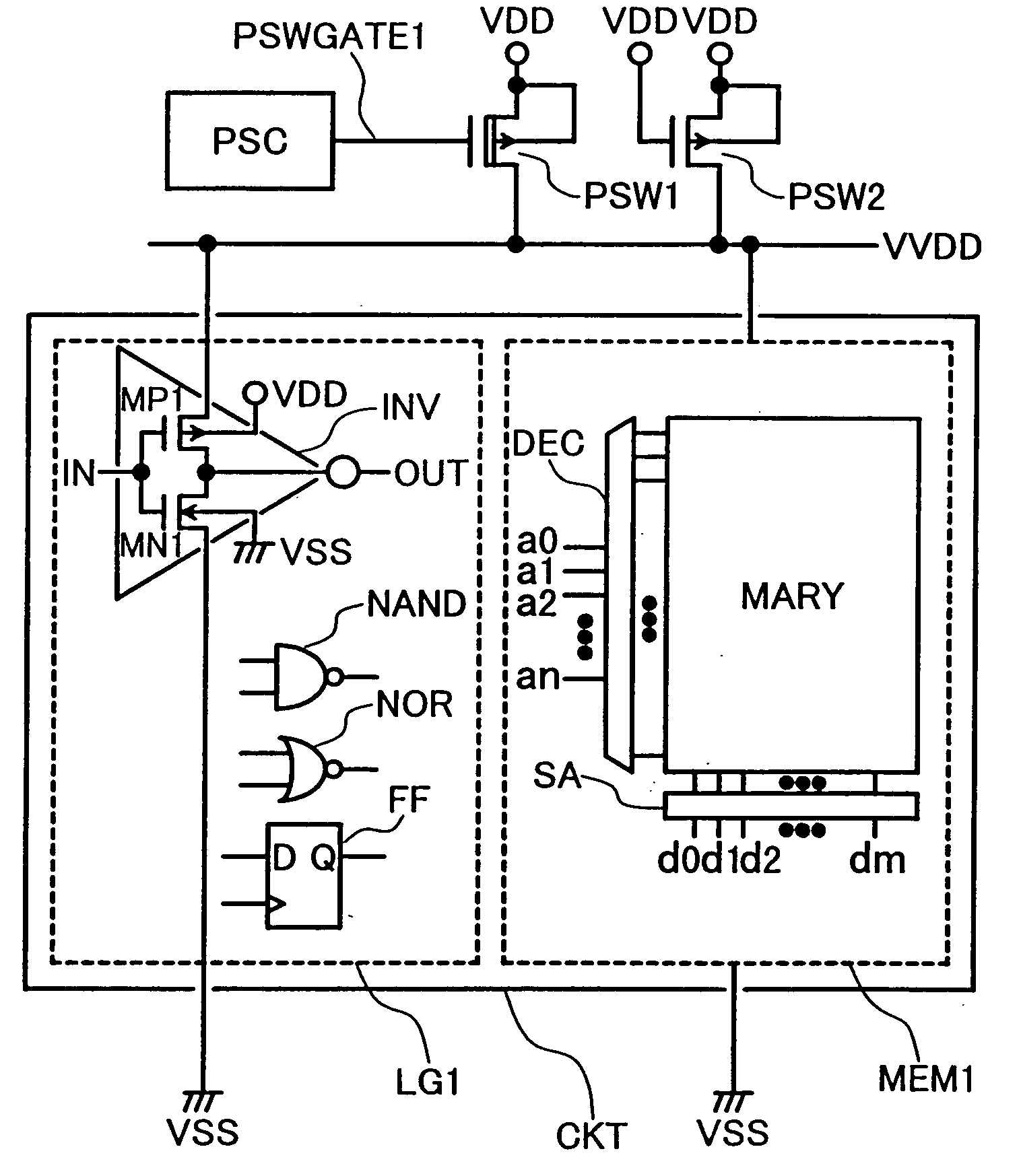
[0053]FIG. 1 is a circuit diagram showing the basic structure of the invention. In the figure, CKT denotes the circuit block, PSW1 denotes the power switch, VDD denotes a power supply voltage for example with a voltage of 1.0 volts, VVDD denotes the virtual power line, VSS denotes the ground with a voltage of 0 volts, and PSC denotes the power switch controller. A circuit block CKT as shown for example in FIG. 1 contains a logic circuit LG1 composed of an inverter INV, a NAND circuit NAND, a NOR circuit NOR and a flip-flop circuit FF; and a memory MEM1 composed of a memory cell array MARY, word decoder DEC and sensing amplifier SA, etc. The circuit block CKT may also be comprised only of a logic circuit LG1 or a memory MEM1. One characteristic feature is it (circuit block) contains information retention circuits such as the flip-flop FF of the logic circuit LG1 and the memory cell array MARY. Here, the information retention circuits are circuits with volatile ...

second embodiment

[0108] Second Embodiment

[0109] Examples of specific circuits applicable to the power control method of the present invention are described next.

[0110]FIG. 31 is a circuit diagram of static memories applicable to the present invention. In the figure, CELL 11 through CELLm1 and CELL1n through CELLmn are static memory cells, BL1 through BLm are the bit lines, / BL1 through / BLm are auxiliary signals for the bit lines BL1 through BLm, and WL1 through WLn are word lines. Here, PS1 through PS2 are virtual power control circuits and include the power switch PSW1 and current source PSW2. The virtual power line connecting the word line WL1 to the memory cells (CEiLL11 through CELLm1) is VL1. The virtual power line connecting the word line WLn to the memory cells (CELL1n through CELLmn) is VLn.

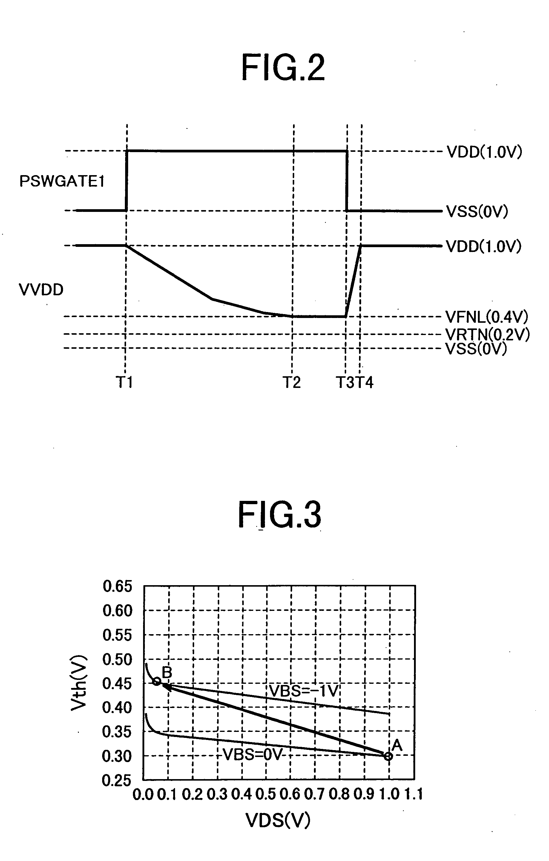
[0111]FIG. 32 is a timing chart for the operation in FIG. 31. The virtual power line VL1 of the memory cell is driven up to the power supply VDD by the virtual power control circuits PS1 at time T1. Af...

third embodiment

[0120] Third Embodiment

[0121]FIG. 35 is a block circuit diagram of the chip CHP1 structure of the present invention. Most of the signal wiring and power supply grounds have been omitted from the drawing for simplicity. The circuit block CKT1 is a circuit block supplied with power directly from a power supply VDD and not by way of the leakage reduction circuit of the present invention. Circuit blocks CKT2a and CKT2b are circuit blocks supplied with power from the power supply VDD by way of the leakage reduction circuits PSM2a and PSM2b of the present invention. The circuit block CKT3 is a circuit block is supplied with power directly from a power supply VCC different from the power supply VDD and not by way of the leakage reduction circuit of the present invention. In the figure, MP20, MP21a, MP22b and MP23 are PMOS transistors. Also in the figure, MN20, MN21a, MN22b, MN23 are NMOS transistors. In the same figure, CTLa, CTLb are leakage control lines of the leakage reduction circuit ...


PUM


Abstract

As the chip manufacturing process progresses towards making smaller and finer chip circuitry, leakage currents of different types including the subthreshold leakage current, gate tunneling leakage current and GIDL (Gate-Induced Drain Leakage) current increase. These leakage currents increase the electrical current consumption of the chip. In a semiconductor integrated circuit device comprising a circuit block having a first MOS transistor, and a leakage current control circuit having a second MOS transistor and a current source, a source and drain circuit of the second MOS transistor is formed between the power supply line of the circuit block and a voltage point where operating voltage is supplied. This current source is connected to the power supply line and in a first state, the power supply line is driven to a first voltage by the second MOS transistor, and in a second state, the power supply line is controlled at a second voltage by current flow in the current source and, the voltage applied across the source and drain of the first MOS transistor in the second state is smaller than the voltage applied across the source and drain of the first MOS transistor in the first state.

Description

FIELD OF THE INVENTION [0001] The present invention relates to a semiconductor integrated circuit device and relates in particular to a semiconductor integrated circuit device with excellent high speed and low power operation characteristics. BACKGROUND OF THE INVENTION [0002] As the chip manufacturing process progresses towards making smaller and finer chip circuitry, the different leakage currents within the chip, including the subthreshold leakage current, gate tunneling leakage current and GIDL (Gate-Induced Drain Leakage) current increase as described in “Identifying defects in deep-submicron CMOS ICs”, IEEE Spectrum, pp. 66-71, September, 1996 (hereafter referred to as reference 1). These leakage currents increase the electrical current consumption of the chip. [0003] A method for reducing subthreshold leakage current in the related art is disclosed in “A Low Power Data Holding Circuit with an Intermittent Power Supply Scheme”, Symposium on VLSI Circuits Digest of Technical Pa...

Claims


Application Information

Patent Timeline
IPC IPC(8): G11C11/413G05F3/26G11C5/14G11C11/407H01L21/822H01L27/04H03K19/00
CPCG05F3/262G11C11/413G11C5/147
Inventor MIZUNO, HIROYUKIITOH, KIYOO
Owner RENESAS ELECTRONICS CORP
Features
  • Generate Ideas
  • Intellectual Property
  • Life Sciences
  • Materials
  • Tech Scout
  • Unparalleled Data Quality
  • Higher Quality Content
  • 60% Fewer Hallucinations
Learn More