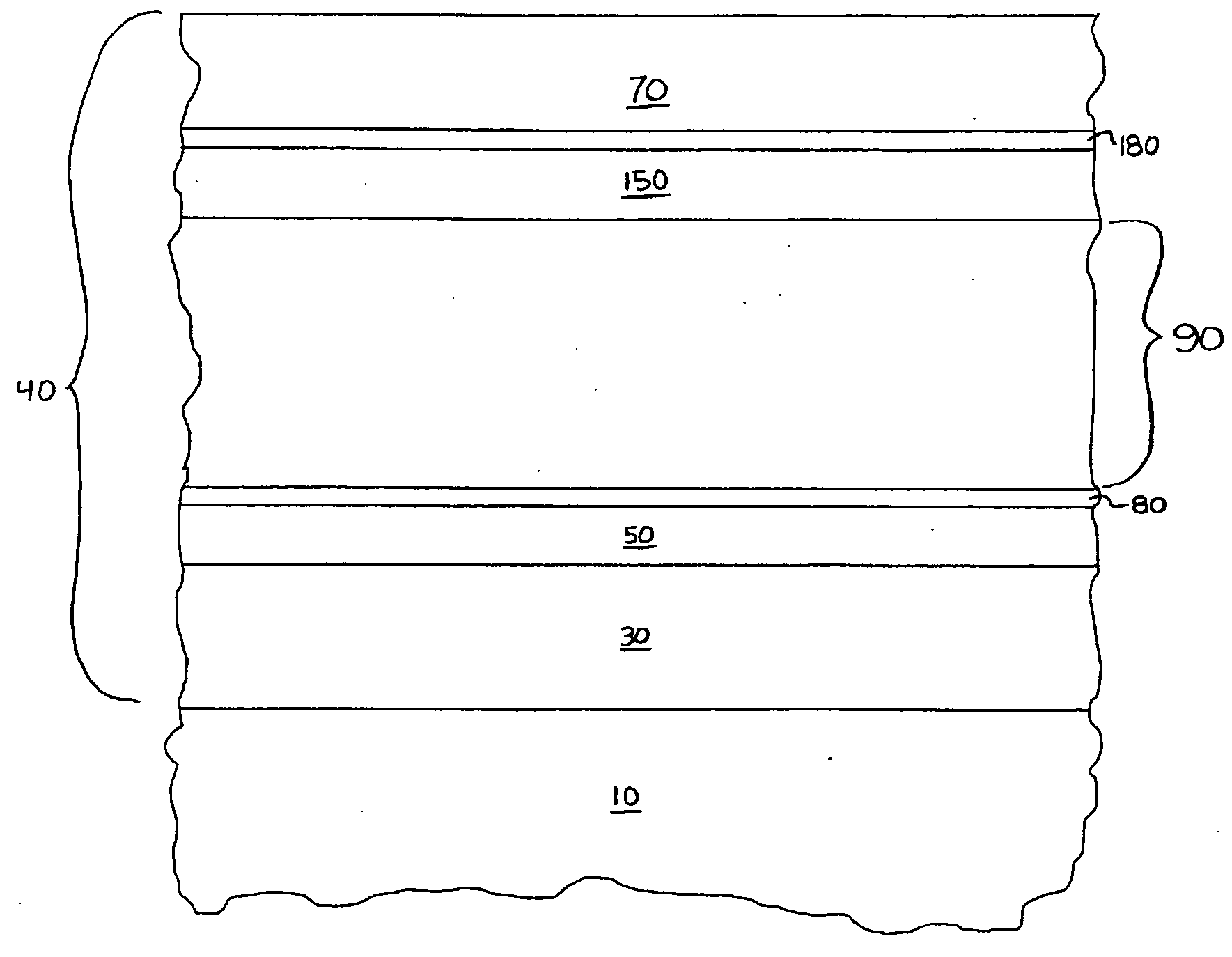
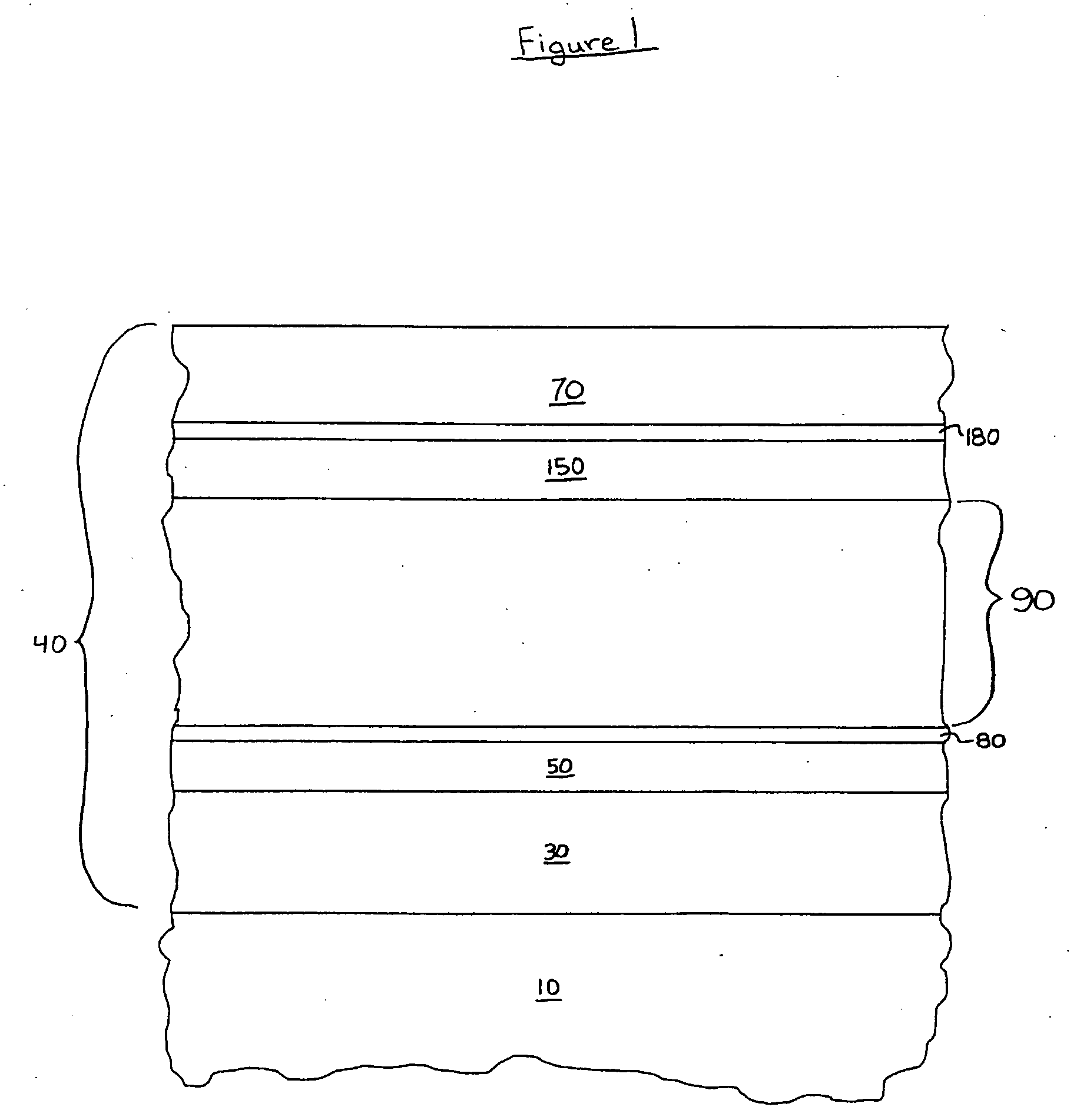
[0017] In certain embodiments, the invention provides a substrate bearing a low-emissivity coating. In these embodiments, the low-emissivity coating comprises, in sequence outwardly: a dielectric inner coat; a first infrared-reflective layer (e.g., comprising material that is highly reflective of solar radiation); a concentration-modulated middle coat including a first graded film region having a substantially continuously decreasing concentration of a first dielectric material and a substantially continuously increasing concentration of a second dielectric material, wherein the first and second dielectric materials are different materials; a second infrared-reflective layer (e.g., comprising material that is highly reflective of solar radiation); and a dielectric outer coat.
[0018] In certain embodiments, the invention provides a substrate bearing a low-emissivity coating. In these embodiments, the low-emissivity coating comprises, in sequence outwardly: a concentration-modulated inner coat including a first graded film region having a substantially continuously decreasing concentration of tin oxide and a substantially continuously increasing concentration of zinc oxide (or zinc tin oxide), wherein the first graded film region extends from a tin oxide-rich inner area to a zinc oxide-rich (or zinc tin oxide-rich) outer area; a first infrared-reflective layer (e.g., comprising material that is highly reflective of solar radiation); a dielectric middle coat; a second infrared-reflective layer (e.g., comprising material that is highly reflective of solar radiation); and a dielectric outer coat.
[0019] In certain embodiments, the invention provides a sputtering line including at least three adjacent sputtering bays each adapted for depositing dielectric film. At least one of these bays is a transition bay equipped with two or more sputtering targets of which at least two carry different sputterable materials. The first target in the transition bay carries the same sputterable material as the last or only target in the preceding (i.e., immediately preceding) bay. The last target in the transition bay carries the same sputterable material as the first or only target in the subsequent (i.e., immediately subsequent) bay.
[0020] In certain embodiments, the invention provides a method of producing coated substrates. In these embodiments, the method comprises providing a sputtering line including at least three adjacent sputtering bays each adapted for depositing dielectric film. At least one of these bays is a transition bay equipped with two or more sputtering targets of which at least two carry different sputterable materials. The first target in the transition bay carries the same sputterable material as the last or only target in the preceding bay. The last target in the transition bay carries the same sputterable material as the first or only target in the subsequent bay. The substrate is conveyed through the sputtering line and the targets are sputtered to deposit upon the substrate a coating comprising a graded film region.
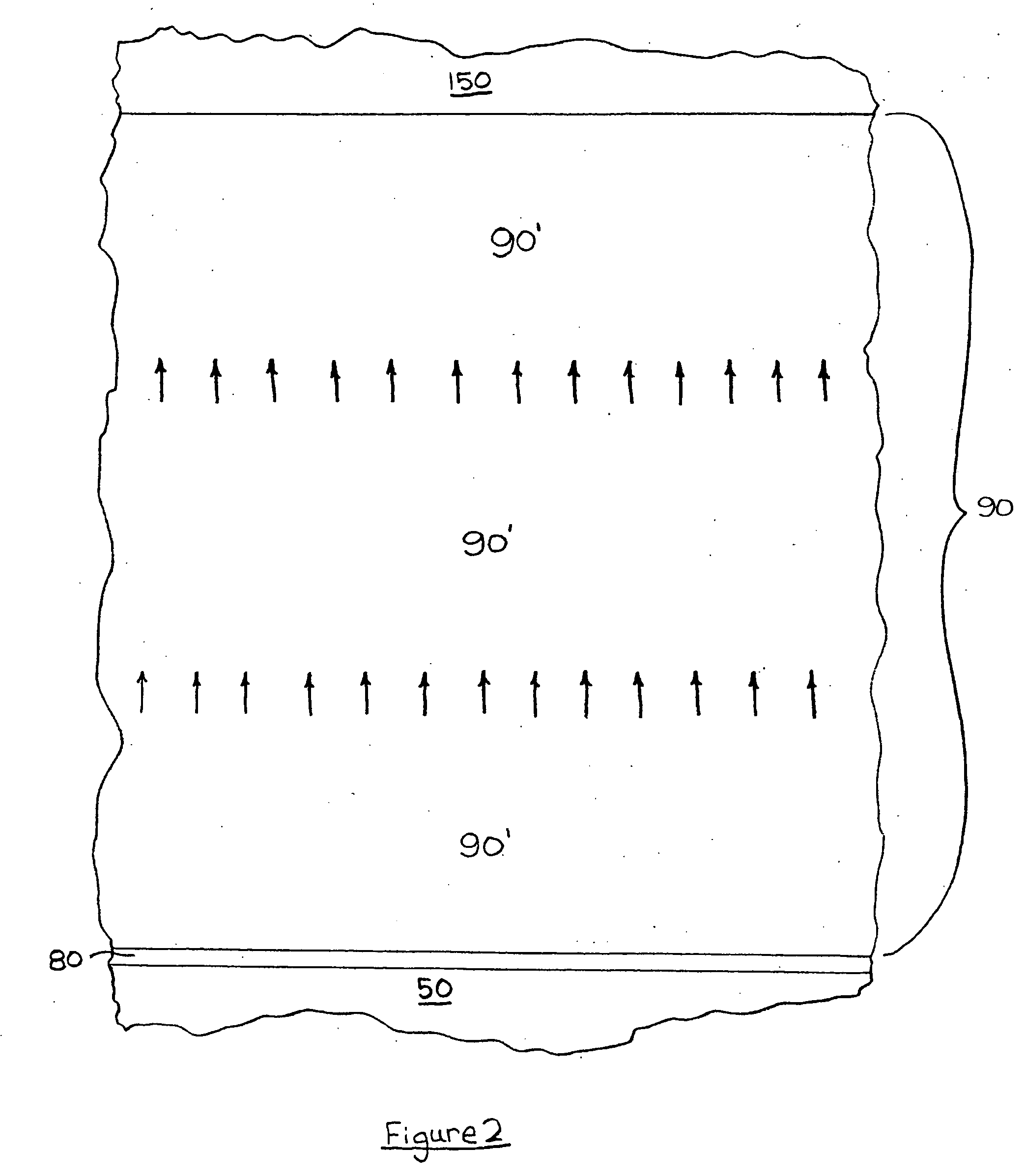
[0021] In certain embodiments, the invention provides a method of producing coated substrates. In these embodiments, the method comprises depositing a low-emissivity coating upon a substrate, the coating comprising, in sequence outwardly: a dielectric inner coat; a first infrared-reflective layer comprising material that is highly reflective of solar radiation; a concentration-modulated middle coat including a first graded film region having a substantially continuously decreasing concentration of a first dielectric material and a substantially continuously increasing concentration of a second dielectric material, wherein the first and second dielectric materials are different materials; a second infrared-reflective layer comprising material that is highly reflective of solar radiation; and a dielectric outer coat. In some cases, the concentration-modulated middle coat is deposited as film having an index of refraction that is substantially uniform across an entire thickness of the middle coat. For example, the concentration-modulated middle coat can be deposited as film having an index of refraction of between about 1.9 and about 2.2. Preferably, the concentration-modulated middle coat is deposited as film wherein there is no discrete interface between homogenous dielectric layers. In some cases, the concentration-modulated middle coat is deposited as film wherein there is no homogenous film region having a thickness of 200 angstroms or more. Preferably, the first graded film region is deposited as film wherein the concentration of the first dielectric material decreases gradually as the concentration of the second dielectric material increases gradually. In some cases, the first dielectric material is tin oxide and the second dielectric material is zinc oxide, and wherein the first graded film region is deposited so as to extend from a tin oxide-rich inner area to a zinc oxide-rich outer area. In these cases, the tin oxide-rich inner area can be deposited directly over a first blocker layer, and the first blocker layer can be deposited directly over the first infrared-reflective layer. This zinc oxide-rich outer area can be deposited as film comprising at least about 40 angstroms of essentially pure zinc oxide directly beneath the second infrared-reflective layer, and the second infrared-reflective layer can be deposited as film comprising silver. In some cases, the concentration-modulated middle coat is deposited as film comprising, in a contiguous sequence moving outwardly: a first high concentration area, the first high concentration area being rich in the first dielectric material; the first graded film region; a second high concentration area, the second high concentration area being rich in the second dielectric material; a second graded film region having a substantially continuously decreasing concentration of the second dielectric material and a substantially continuously increasing concentration of a third dielectric material, wherein the second and third dielectric materials are different materials; and a third high concentration area, the third high concentration area being rich in the third dielectric material. In these cases, the third dielectric material can be zinc oxide, such that the third high concentration area is deposited as a zinc oxide-rich area. This zinc oxide-rich area can be deposited as film comprising at least about 40 angstroms of essentially pure zinc oxide directly beneath the second infrared-reflective layer, and the second infrared-reflective layer can be deposited as film comprising silver. The first and third dielectric materials can both the same material, if so desired, such that the first and third high concentration areas are both deposited as film rich in the same material. For example, the first and third dielectric materials can both be zinc oxide, such that the first and third high concentration areas are both deposited as zinc oxide-rich areas. Further, the second dielectric material can be deposited as an oxide selected from the group consisting of tin oxide, zinc tin oxide, and titanium oxide. In some cases, the first high concentration area is deposited as film comprising a first homogenous film region consisting essentially of the first dielectric material, the second high concentration area is deposited as film comprising a second homogenous film region consisting essentially of the second dielectric material, and the third high concentration area is deposited as film comprising a third homogenous film region consisting essentially of the third dielectric material. In these cases, each homogenous film region is preferably deposited at a thickness of less than 200 angstroms. Further, the second homogenous film region is preferably deposited at a thickness of less than about 180 angstroms. In some cases, the concentration-modulated middle coat is deposited as film comprising, in a contiguous sequence moving outwardly: a first high concentration area, the first high concentration area being rich in the first dielectric material; the first graded film region; a second high concentration area, the second high concentration area being rich in the second dielectric material; a second graded film region having a substantially continuously decreasing concentration of the second dielectric material and a substantially continuously increasing concentration of a third dielectric material, wherein the second and third dielectric materials are different materials; a third high concentration area, the third high concentration area being rich in the third dielectric material; a third graded film region having a substantially continuously decreasing concentration of the third dielectric material and a substantially continuously increasing concentration of a fourth dielectric material, wherein the third and fourth dielectric materials are different materials; a fourth high concentration area, the fourth high concentration area being rich in the fourth dielectric material; a fourth graded film region having a substantially continuously decreasing concentration of the fourth dielectric material and a substantially continuously increasing concentration of a fifth dielectric material, wherein the fourth and fifth dielectric materials are different materials; and a fifth high concentration area, the fifth high concentration area being rich in the fifth dielectric material. Preferably, the fifth dielectric material is zinc oxide, such that the fifth high concentration area is deposited as a zinc oxide-rich area. This zinc oxide-rich area can be advantageously deposited as film comprising at least about 40 angstroms of essentially pure zinc oxide directly beneath the second infrared-reflective layer, and the second infrared-reflective layer can be advantageously deposited as film comprising silver. If so desired, the first, third, and fifth dielectric materials can all be the same material, such that the first, third, and fifth high concentration areas are all deposited as film rich in the same material. For example, the first, third, and fifth dielectric materials can all be zinc oxide, such that the first, third, and fifth high concentration areas are all deposited as zinc oxide-rich areas. Further, the second and fourth dielectric materials can both be the same material, such that the second and fourth high concentration areas are both deposited as film rich in the same material. For example, the second and fourth dielectric materials can both be deposited as an oxide selected from the group consisting of tin oxide, zinc tin oxide, and titanium oxide. In some cases, the first high concentration area is deposited as film comprising a first homogenous film region consisting essentially of the first dielectric material, the second high concentration area is deposited as film comprising a second homogenous film region consisting essentially of the second dielectric material, the third high concentration area is deposited as film comprising a third homogenous film region consisting essentially of the third dielectric material, the fourth high concentration area is deposited as film comprising a fourth homogenous film region consisting essentially of the fourth dielectric material, and the fifth high concentration area is deposited as film comprising a fifth homogenous film region consisting essentially of the fifth dielectric material. Preferably, each homogenous film region is deposited at a thickness of less than 200 angstroms. Further, the second and fourth homogenous film regions are preferably each deposited at a thickness of less than about 180 angstroms. In some cases, the dielectric inner coat is deposited as a concentration-modulated inner coat comprising a second graded film region having a substantially continuously decreasing concentration of a third dielectric material and a substantially continuously increasing concentration of a fourth dielectric material, wherein the third and fourth dielectric materials are different materials. Additionally (or alternatively), the dielectric outer coat can be deposited as a concentration-modulated outer coat comprising a third graded film region having a substantially continuously decreasing concentration of a fifth dielectric material and a substantially continuously increasing concentration of a sixth dielectric material, wherein the fifth and sixth dielectric materials are different materials. In some cases of this nature, the concentration-modulated inner, middle, and outer coats are each deposited as film not including any discrete interface between homogenous dielectric layers.
[0022] In certain embodiments, the invention provides a method of producing coated substrates. In these embodiments, the method comprises depositing a low-emissivity coating upon a substrate, the coating comprising, in sequence outwardly: a concentration-modulated inner coat including a first graded film region having a substantially continuously decreasing concentration of tin oxide and a substantially continuously increasing concentration of zinc oxide or zinc tin oxide, wherein the first graded film region extends from a tin oxide-rich inner area to a zinc oxide-rich or zinc tin oxide-rich outer area; a first infrared-reflective layer comprising material that is highly reflective of solar radiation; a dielectric middle coat; a second infrared-reflective layer comprising material that is highly reflective of solar radiation; and a dielectric outer coat. Preferably, the tin oxide-rich inner area of the first graded film region is deposited as film consisting essentially of tin oxide. In some cases, the tin oxide-rich inner portion of the first graded film region is deposited directly over the substrate. In other cases, the low-emissivity coating further includes a base layer comprising silicon dioxide deposited directly over the substrate, the tin oxide-rich inner area of the first graded film region being deposited directly over the base layer. Preferably, the first infrared-reflective layer is deposited directly over the outer area of the first graded film region. The outer area of the first graded film region can be advantageously deposited as film comprising at least about 40 angstroms of essentially pure zinc oxide directly beneath the first infrared-reflective layer, and the first infrared-reflective layer can be advantageously deposited as film comprising silver. In some cases, the concentration-modulated inner coat is deposited as film comprising, in a contiguous sequence moving outwardly: a first high concentration area, the first high concentration area being rich in tin oxide; the first graded film region; a second high concentration area, the second high concentration area being rich in zinc oxide or zinc tin oxide; a second graded film region having a substantially continuously decreasing concentration of zinc oxide or zinc tin oxide and a substantially continuously increasing concentration of tin oxide; a third high concentration area, the third high concentration area being rich in tin oxide; a third graded film region having a substantially continuously decreasing concentration of tin oxide and a substantially continuously increasing concentration of zinc oxide or zinc tin oxide; and a fourth high concentration area, the fourth high concentration area being rich in zinc oxide or zinc tin oxide.

