Precise patterning of high-k films
- Summary
- Abstract
- Description
- Claims
- Application Information
AI Technical Summary
Benefits of technology
Problems solved by technology
Method used
Image

Examples
Embodiment Construction
[0009] In the following detailed description of embodiments of the invention, reference is made to the accompanying drawings in which like references indicate similar elements. The illustrative embodiments described herein are disclosed in sufficient detail to enable those skilled in the art to practice the invention. The following detailed description is therefore not to be taken in a limiting sense, and the scope of the invention is defined only by the appended claims.
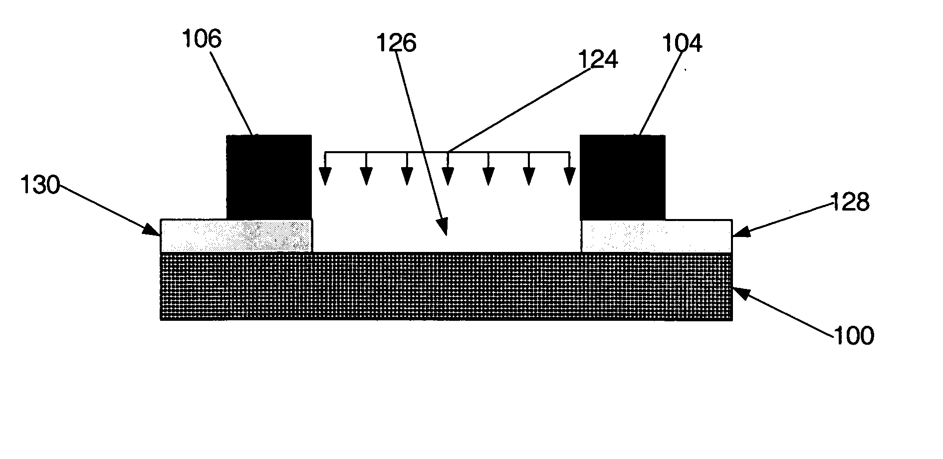
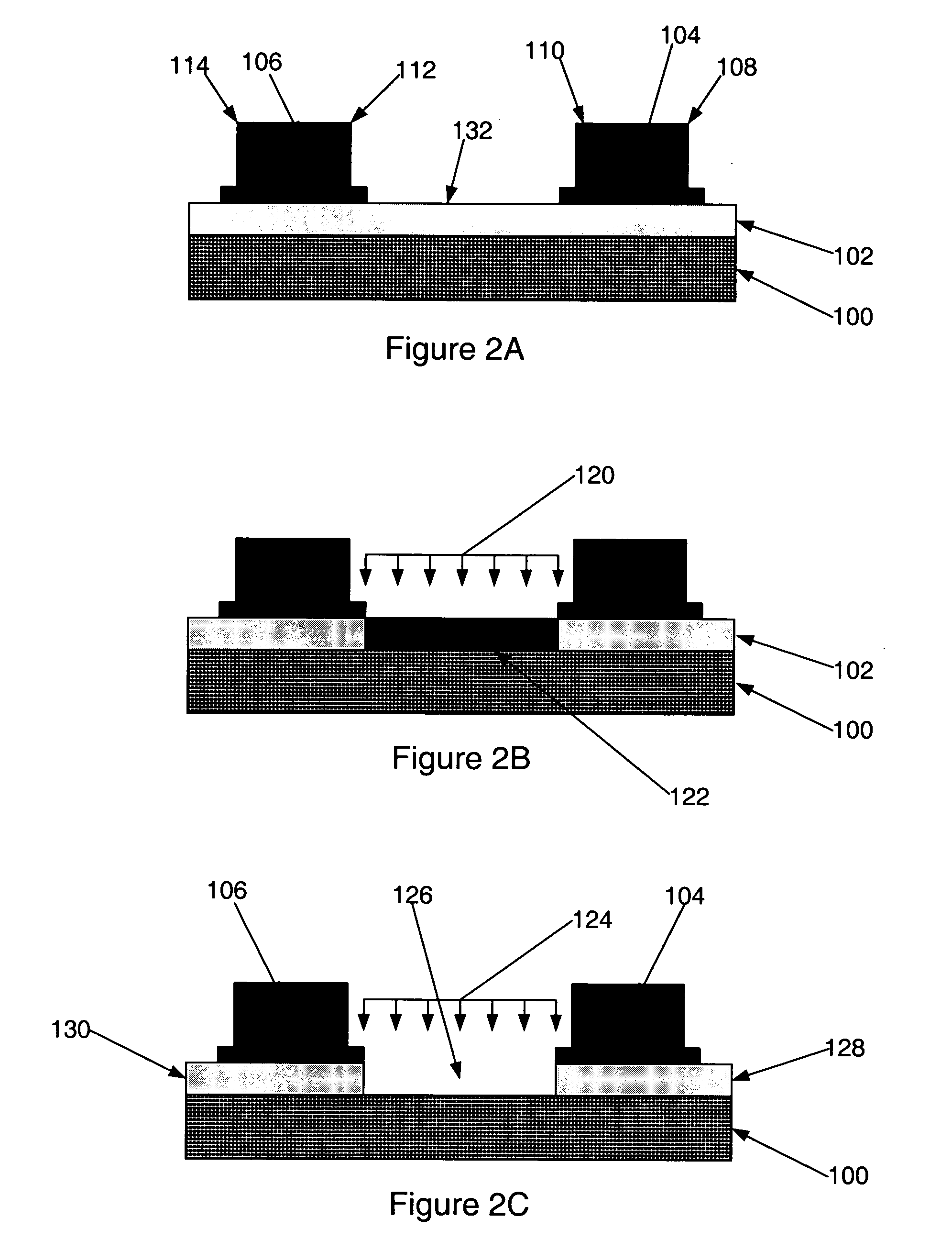
[0010]FIGS. 2A-2C are cross sectional views of various aspects of a patterning treatment of one embodiment of the present invention. Referring to FIG. 2A, a microelectronic structure similar to that depicted in FIG. 1A is shown. Such a structure may be formed utilizing various techniques and materials. For example, a high-K dielectric layer (102) may be formed upon a substrate layer (100) using techniques such as chemical or physical vapor deposition or other techniques. In various embodiments, the high-K dielectric...
PUM
 Abstract
Description
Claims
Application Information
 - R&D Engineer
- R&D Manager
- IP Professional
- Industry Leading Data Capabilities
- Powerful AI technology
- Patent DNA Extraction
Browse by: Latest US Patents, China's latest patents, Technical Efficacy Thesaurus, Application Domain, Technology Topic.
© 2024 PatSnap. All rights reserved.Legal|Privacy policy|Modern Slavery Act Transparency Statement|Sitemap