SDRAM memory device with an embedded NAND flash controller

a memory device and controller technology, applied in the field of memory devices, can solve the problems of slow writing, random access, slow writing, etc., and achieve the effect of slow writing (a few microseconds, erasing must be done,

Inactive Publication Date: 2005-02-03
INNOVATIVE MEMORY SYST INC
View PDF16 Cites 258 Cited by
  • Summary
  • Abstract
  • Description
  • Claims
  • Application Information

AI Technical Summary

Problems solved by technology

Writing also is random access but is slow (a few microseconds).
Erasing must be done in large chunks called “blocks” and is very slow (a few hundred milliseconds).
Writing must be done in medium-size chunks called “pages” and is slow (a few hundred microseconds).
Unlike NOR flash, in which reading is random access, NAND flash does not support execution-in-place, such as is needed to boot the host system.

Method used


Image

  • SDRAM memory device with an embedded NAND flash controller
  • SDRAM memory device with an embedded NAND flash controller
  • SDRAM memory device with an embedded NAND flash controller

Examples


Embodiment Construction

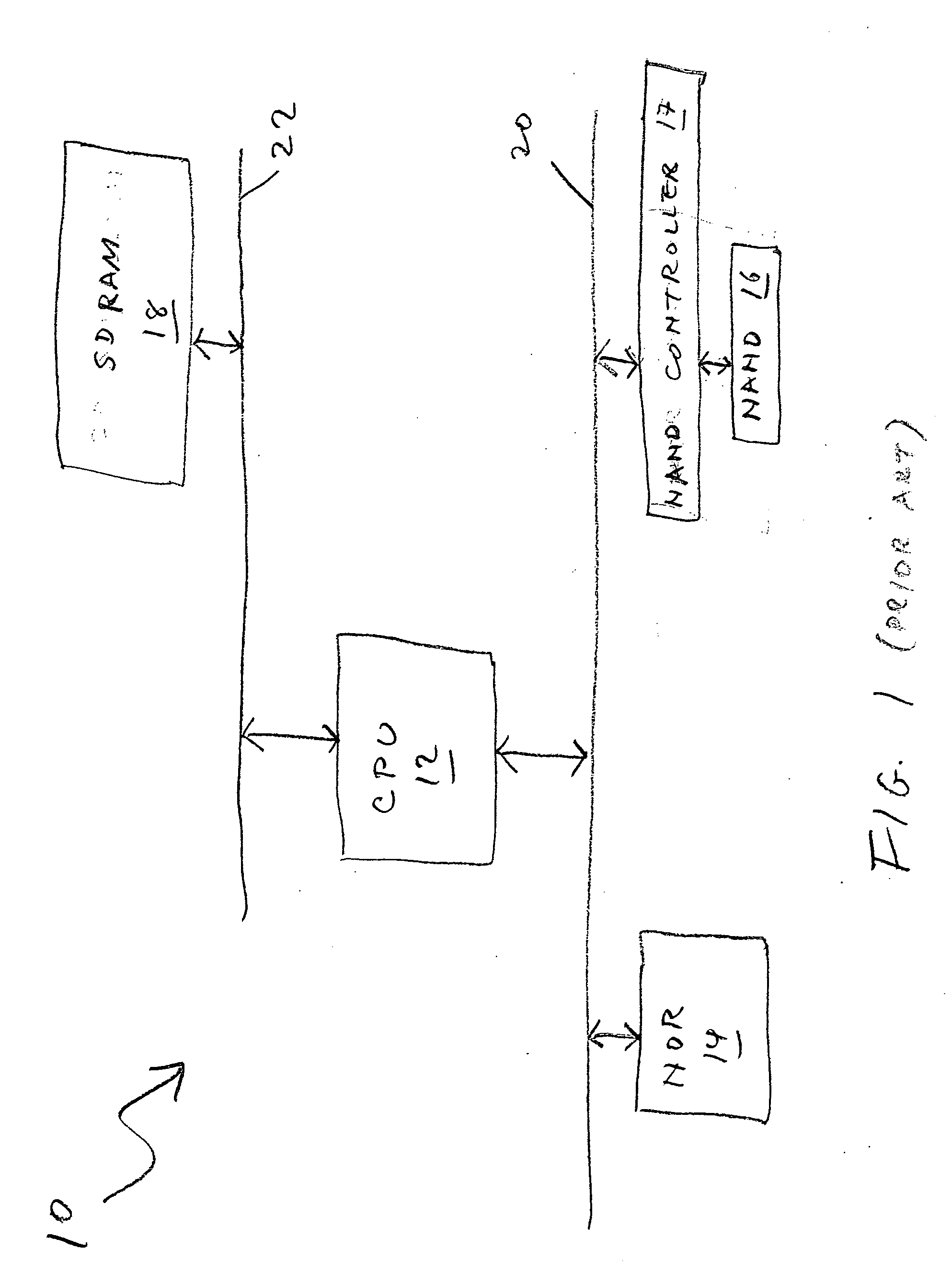
[0075] The present invention is of a memory device that includes two kinds of memories but communicates with a host device or system using the protocol and signals of only one of the memories. The present invention thereby enables the host device or system to include only one bus for communicating with the two memories.

[0076] The principles and operation of a memory device according to the present invention may be better understood with reference to the drawings and the accompanying description.

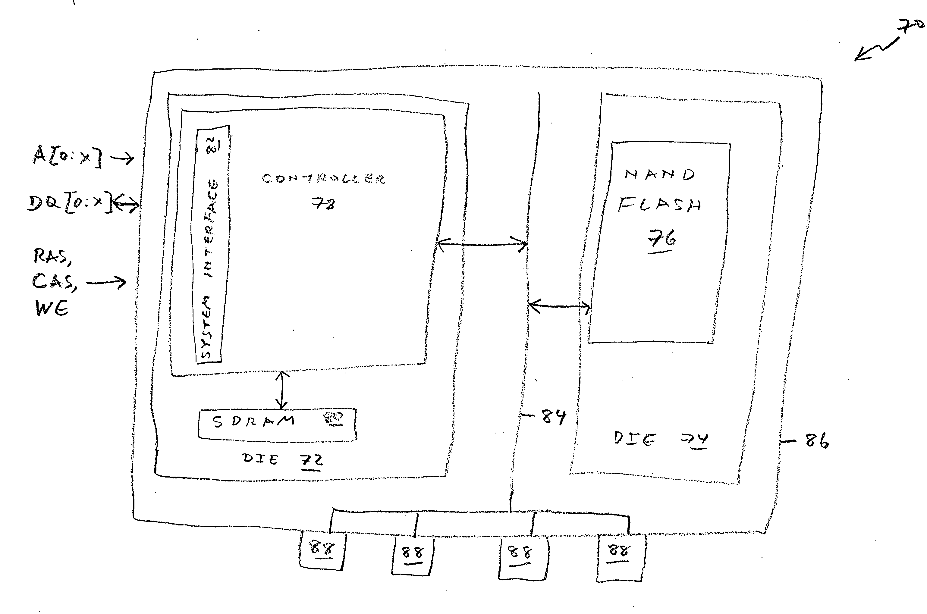
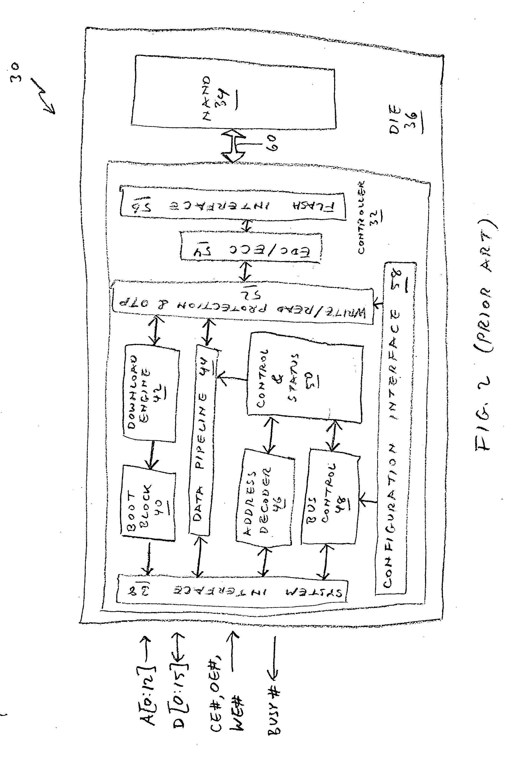
[0077] Returning now to the drawings, FIG. 3 is a high-level block diagram of a memory device 70 of the present invention. Device 70 includes two dies 72 and 74. Fabricated on die 74 is a NAND flash memory 76. Fabricated on die 72 are a controller 78 for NAND flash memory 76 and a SDRAM 80. Controller 78 is similar to prior art controller 32. There are three principal differences between controller 78 and controller 32. The first difference is that in addition to communicating with NAND fla...


PUM


Abstract

A memory device includes two dies. A first memory is fabricated on one die. A controller of the first memory is fabricated on the other die. Also fabricated on the other die is another component, such as a second memory, that communicates with a host system using a plurality of signals different from the signals used by the first memory. The device includes a single interface for communicating with the host system using only the respective signals of the second component. In a most preferred embodiment, the first memory is a NAND flash memory and the second memory is a SDRAM.

Description

[0001] This is a continuation-in-part of U.S. Provisional Patent Application Ser. No. 60 / 492,217, filed on Jul. 31, 2003.FIELD AND BACKGROUND OF THE INVENTION [0002] The present invention relates to memory devices and, more particularly, to a MCP (multi-chip package) memory device with a NAND flash memory on one die and a SDRAM (synchronous dynamic random access memory) together with a controller for the NAND flash memory on another die. [0003]FIG. 1 is a partial high level block diagram of a generic prior art embedded device 10. Device 10 includes a central processing unit (CPU) 12 and three memory devices 14, 16 and 18. Memory device 14 includes a nonvolatile memory such as a NOR flash memory for storing the operating system and the pre-stored applications of device 10. Memory device 16 includes a nonvolatile memory such as a NAND flash memory accessed via a NAND controller 17, for storing the user's data and downloaded applications. Memory device 18 is a volatile memory Such as a...

Claims


Application Information

Patent Timeline
Patent Type & Authority Applications(United States)
IPC IPC(8): G06FG06F12/00G06F13/28G11C5/00G11C14/00
CPCG06F9/4403G06F9/4406G11C14/0018G11C14/00G06F9/44573G06F12/00G06F13/20G06F13/28
Inventor AVRAHAM, MEIRINBAR, DANPAZ, ZIV
Owner INNOVATIVE MEMORY SYST INC
Why Eureka
Try Eureka