Light-emitting diode lamp

a diode lamp and light-emitting technology, applied in the field of light-emitting diode lamps, can solve the problems of increasing manufacturing costs, and achieve the effect of achieving stable solder-joint performan

Inactive Publication Date: 2005-02-10
TOYODA GOSEI CO LTD +1
View PDF8 Cites 27 Cited by
  • Summary
  • Abstract
  • Description
  • Claims
  • Application Information

AI Technical Summary

Benefits of technology

[0020] According to one aspect of the present invention, the solder-flowing recess for inflow of the solder is formed between the terminal portion of the lamp and the outside thereof to enable supply of an appropriate amount of the solder, so that stable solder-joint performance can be easily obtained.

Problems solved by technology

Therefore, it is required to maintain a formation stability of the bump at a certain level for a good solder-joint performance, and as a result, a problem with an increase of manufacturing costs occurs.

Method used


Image

  • Light-emitting diode lamp
  • Light-emitting diode lamp
  • Light-emitting diode lamp

Examples


first embodiment

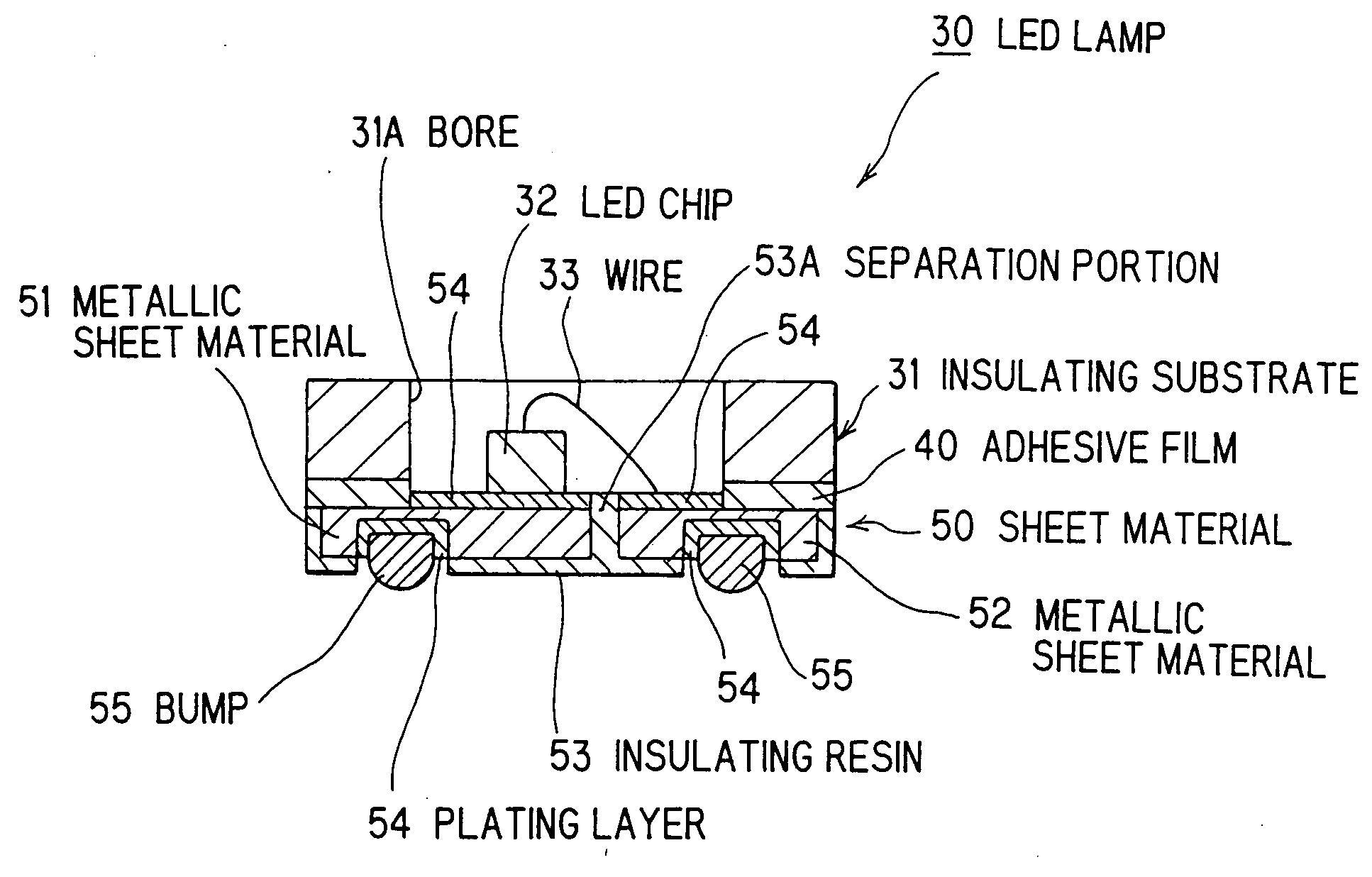
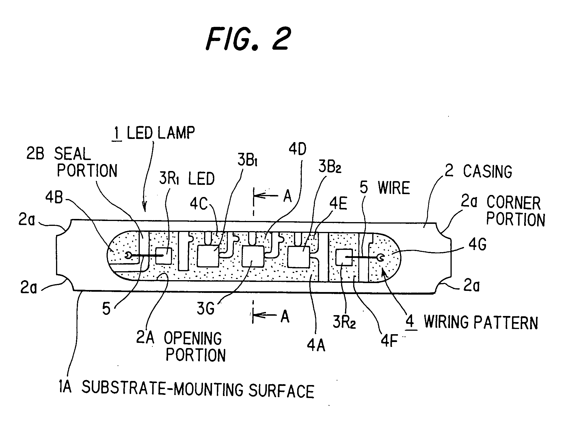
[0035]FIG. 2 is a front view of a light-emitting diode lamp of a first embodiment according to the present invention. The light-emitting diode lamp 1 is provided with a casing 2 formed of laminating sheet materials, an array of light-emitting diodes (referred to as LED hereinafter) 3R1, 3R2, 3G, 3B1, and 3B2 received in an oval opening portion 2A of the case 2, and wiring patterns 4 disposed in a substrate to be described later for electrically connecting the LEDs, and the opening portion 2A is filled with a transparent epoxy resin as a seal resin to form a seal portion 2B, which protects each LED.

[0036] The casing 2 is formed by laminating a plurality of ceramic sheet materials where the LEDs 3R1, 3R2, 3G, 3B1, and 3B2 are arranged in an array in the oval opening portion 2A to form a LED lamp. And the casing 2 includes corner portions 2a, each having a shape of an inverted arc.

[0037] The LEDs 3R1, 3R2 (red color) have electrodes on the upper surface and the bottom surface thereof...

second embodiment

[0068]FIG. 8A is a perspective view of a light-emitting apparatus 1A of a second embodiment. FIG. 8B is a partially enlarged view of a solder-flowing recess SFR. This perspective view is a bottom-side perspective view opposite the light-emitting direction of the light-emitting diode lamp 1 mounted on the outside substrate 8. However, components identical to those in the first embodiment are referred to the same numbers.

[0069] According to the second embodiment, the solder-flowing recess SFR includes recess-shaped groove portions 9A formed in wiring patterns 9 of the outside substrate 8 and the notch portions 7A of the wiring patterns 7. The groove portions 9A are disposed opposite to the notch portions 7A, but each of the groove portions 9A, as shown in FIG. 8B, is arranged deviated by a length 1 from each of the notch portions 7A. Such groove portions 9A can be produced by partially removing the wiring patterns 9 and the outside substrate 8 by etching or the like.

[0070] According...

third embodiment

[0075]FIG. 9A is a perspective view of a light-emitting apparatus 1B of a third embodiment. FIG. 9B is a partially enlarged view of a groove portion as a solder-flowing recess. This perspective view is a bottom-side perspective view which is opposite the light-emitting direction of the light-emitting diode lamp 1 mounted on the outside substrate 8.

[0076] The third embodiment is constructed such that the groove portions 9A are disposed in the wiring patterns 9 without providing the wiring patterns 7 with any notch portion, which also prevents a large number of the solders from moving up.


PUM


Abstract

A notch portion 7A is disposed on a formation surface of a wiring pattern 7 and is located in a contact point with a wiring pattern 9 of an outside substrate 8, so that a solder 9a melted by reflow soldering slowly flows up along an edge of the notch portion 7A, improving a solder-joint performance. The notch portion 7A is formed in a recess shape as formed by cutting away the substrate 6 and as a result, the melted solder stays in the recess portion, which prevents the melted solder from moving up over the notch portion 7A.

Description

[0001] The present application is based on Japanese patent application No. 2003-288294, the entire contents of which are incorporated herein by reference. BACKGROUND OF THE INVENTION [0002] 1. Field of the Invention [0003] The present invention relates to a light-emitting diode lamp and in particular to a light-emitting diode lamp adapted to regulate flow of solder in soldering. [0004] 2. The Related Art of the Invention [0005] There is known a light-emitting lamp that has a light-emitting diode (to be referred to as LED hereinafter) as a light source. Such light-emitting lamp has an advantage that use of the LED as a light source allows the lamp to have a good lighting performance with a low electrical power consumption, as well as an excellent mounting performance in mounting the lamp to various electronic devices requiring a light source. [0006] Recent progress in miniaturization of an electric device or the like requires further miniaturization of a light-emitting lamp, which ra...

Claims


Application Information

Patent Timeline
Patent Type & Authority Applications(United States)
IPC IPC(8): H01L23/12H01L25/075H01L33/48H05K3/34
CPCF21K99/00H01L25/0753H05K3/3442H05K2201/10106H05K2201/1084H01L2224/48227H05K2201/10931H01L2224/48091H01L2924/00014Y02P70/50
Inventor KATO, HIDEAKIMATSUMURA, KANAEOHTSUKA, SHUNSUKE
Owner TOYODA GOSEI CO LTD
Why Eureka
Try Eureka