Method for fabricating pattern, apparatus for fabricating pattern, conductive film wiring, method for fabricating device, electro-optical apparatus, and electronic apparatus

a technology of conductive film and pattern, applied in the direction of identification means, instruments, discharge tube coating, etc., can solve the problems of reducing the performance of the pattern, affecting the shape of the pattern, and difficulty in broadening the width of the film pattern, etc., to achieve the effect of preferable shap

Inactive Publication Date: 2005-02-17
SEIKO EPSON CORP
View PDF12 Cites 1 Cited by
  • Summary
  • Abstract
  • Description
  • Claims
  • Application Information

AI Technical Summary

Benefits of technology

[0009] The present invention was conceived in view of the above circumstances, and the present invention provides a method...

Problems solved by technology

In addition, this process is applicable even to a large substrate that may be difficult to handle in the spin coating process.
However, the process, in which a liquid material is disposed as liquid droplets onto a substrate, encounters a problem in that it is difficult to broaden the width of the film pattern.
More specifically, when the volume of ...

Method used


Image

  • Method for fabricating pattern, apparatus for fabricating pattern, conductive film wiring, method for fabricating device, electro-optical apparatus, and electronic apparatus
  • Method for fabricating pattern, apparatus for fabricating pattern, conductive film wiring, method for fabricating device, electro-optical apparatus, and electronic apparatus
  • Method for fabricating pattern, apparatus for fabricating pattern, conductive film wiring, method for fabricating device, electro-optical apparatus, and electronic apparatus

Examples


Embodiment Construction

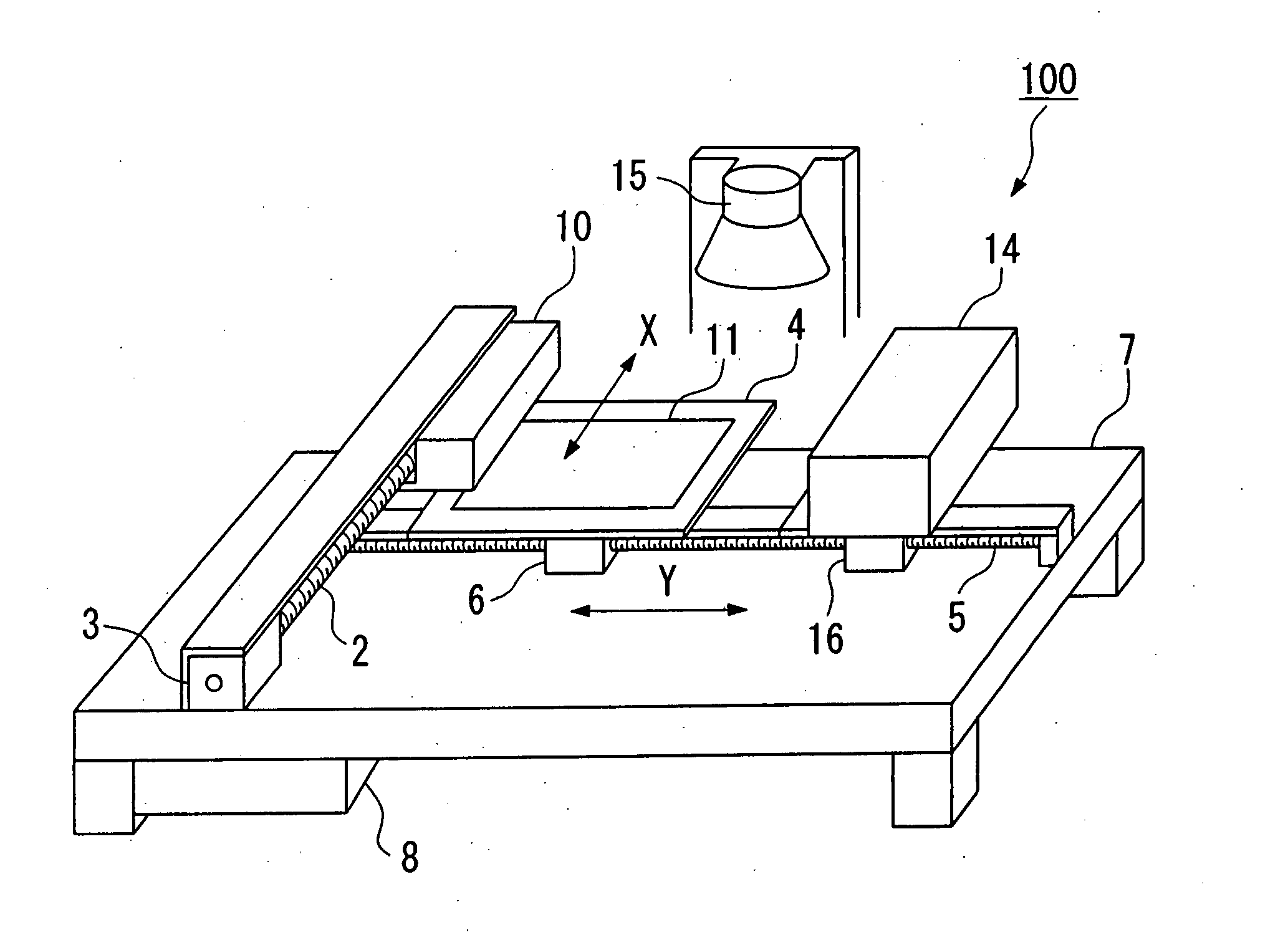
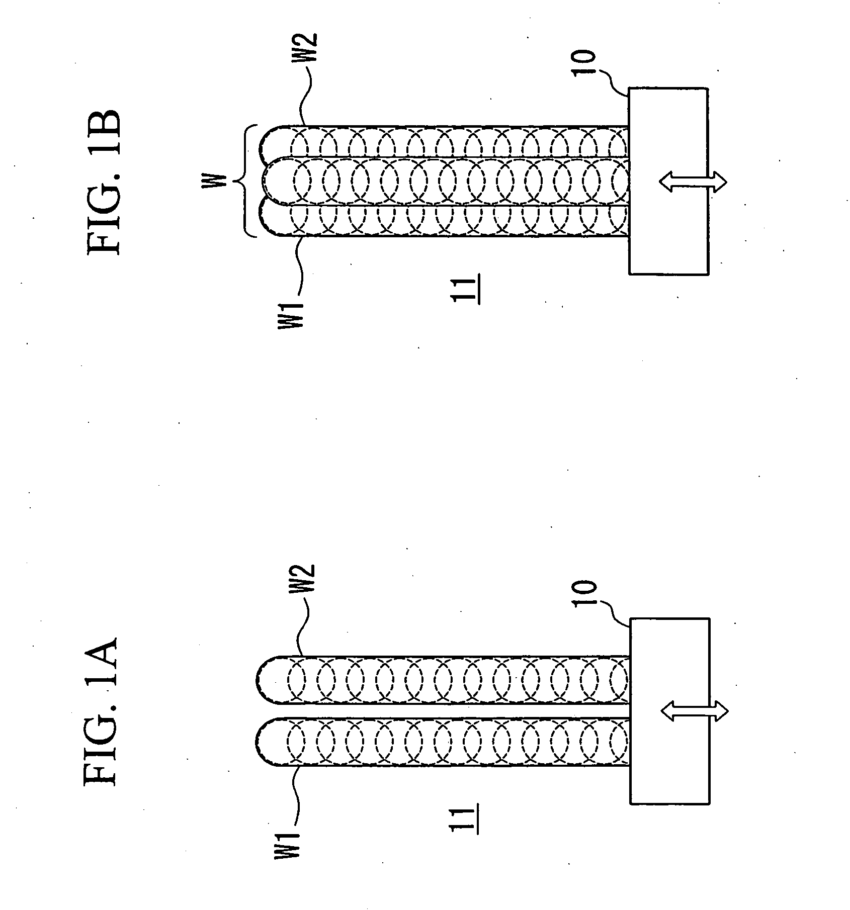
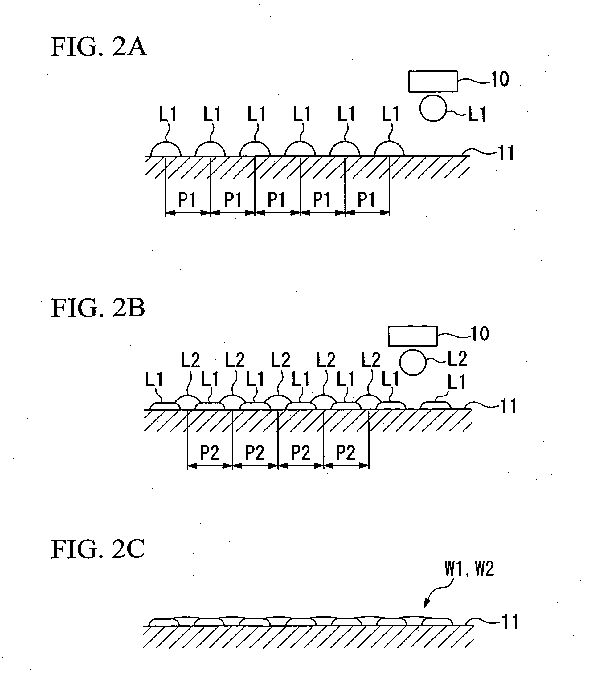
[0049] Next, a method for fabricating a conductive film wiring on a substrate, which is as an example of the embodiments of the present invention, will be explained. In the method for fabricating a wiring according to the present embodiment, a liquid material for forming a conductive film wiring is disposed on a substrate, and a conductive film pattern for wiring is fabricated on the substrate. The method includes a surface treatment process, a material disposing process, and a heat treatment and optical treatment process. Disposing of the liquid material is conducted using a liquid droplet ejecting device, by which a liquid disposing process, i.e., a so-called ink-jet process, in which the liquid material is ejected as liquid droplets from nozzles of an ejecting head, is carried out. The ejecting method employed in the liquid droplet ejecting device may be a piezo-jet method in which a liquid material (fluid) is ejected due to a volume change of a piezoelectric element, a method in...


PUM


Abstract

A method and an apparatus for fabricating a pattern which makes it possible to obtain a wide pattern having edges of a preferable shape. The apparatus for fabricating a pattern ejects a liquid material as liquid droplets from an ejecting section, and dispose the liquid droplets on a substrate in a line-shaped pattern. A plurality of line-shaped patterns are formed on the substrate by disposing a plurality of liquid droplets on the substrate in the line-shaped patterns, and then another set of liquid droplets are disposed between the line-shaped patterns so as to integrate the line-shaped patterns with each other.

Description

[0001] This is a Division of application Ser. No. 10 / 409,210 filed Apr. 9, 2003. The entire disclosure of the prior application is hereby incorporated by reference herein in its entirety.BACKGROUND OF THE INVENTION [0002] 1. Field of the Invention [0003] The present invention relates to a method and an apparatus for fabricating a pattern on a substrate, in particular, the present invention relates to a process for fabricating a pattern on a substrate by ejecting a liquid material in the form of liquid droplets from a liquid droplet ejecting section. [0004] 2. Background Art [0005] As a process for fabricating a pattern on a substrate, a process is known in which a film of liquid material for fabricating a pattern is formed on a substrate using a coating process such as the spin coat process, and the film is fabricated into a desired pattern using the photolithography process. [0006] On the other hand, another process has been proposed in which a liquid material is disposed at desire...

Claims


Application Information

Patent Timeline
IPC IPC(8): B05D1/26H05B33/10B05D7/00B41J2/07B41J3/407B41J11/00B41J29/00G02F1/13G09F9/00H01L21/00H01L21/288H01L21/3205H01L21/48H01L21/768H01L51/40H01L51/50H05K3/12
CPCB41J3/407B41J11/008H01L2924/0002B41M3/001B41M3/16H01J2209/012H01J2217/49207H01L21/288H01L21/4867H01L21/67138H01L21/6715H01L21/76838H01L51/0004H05K3/125H01L2924/00H10K71/13B41J29/00
Inventor HASEI, HIRONORI
Owner SEIKO EPSON CORP
Why Eureka
Try Eureka