Method of forming a pattern and substrate processing system

a processing system and substrate technology, applied in the direction of coatings, chemical vapor deposition coatings, electric discharge tubes, etc., can solve the problems of reducing the aspect ratio of substrates and the inability to obtain desired semiconductor device properties, and achieve the effect of preferable shap

Active Publication Date: 2016-03-08
TOKYO ELECTRON LTD
View PDF9 Cites 0 Cited by
  • Summary
  • Abstract
  • Description
  • Claims
  • Application Information

AI Technical Summary

Benefits of technology

[0011]According to an embodiment of the present invention, a pattern having a preferable shape can be formed on a substrate.

Problems solved by technology

Moreover, when a side wall of the hole is etched as well as the bottom of the hole during the etching, an aspect ratio thereof decreases because of an increased critical dimension value (Critical Dimension) that is a diameter of the top of the hole, and desired semiconductor device properties cannot be obtained.

Method used


Image

  • Method of forming a pattern and substrate processing system
  • Method of forming a pattern and substrate processing system
  • Method of forming a pattern and substrate processing system

Examples


first embodiment

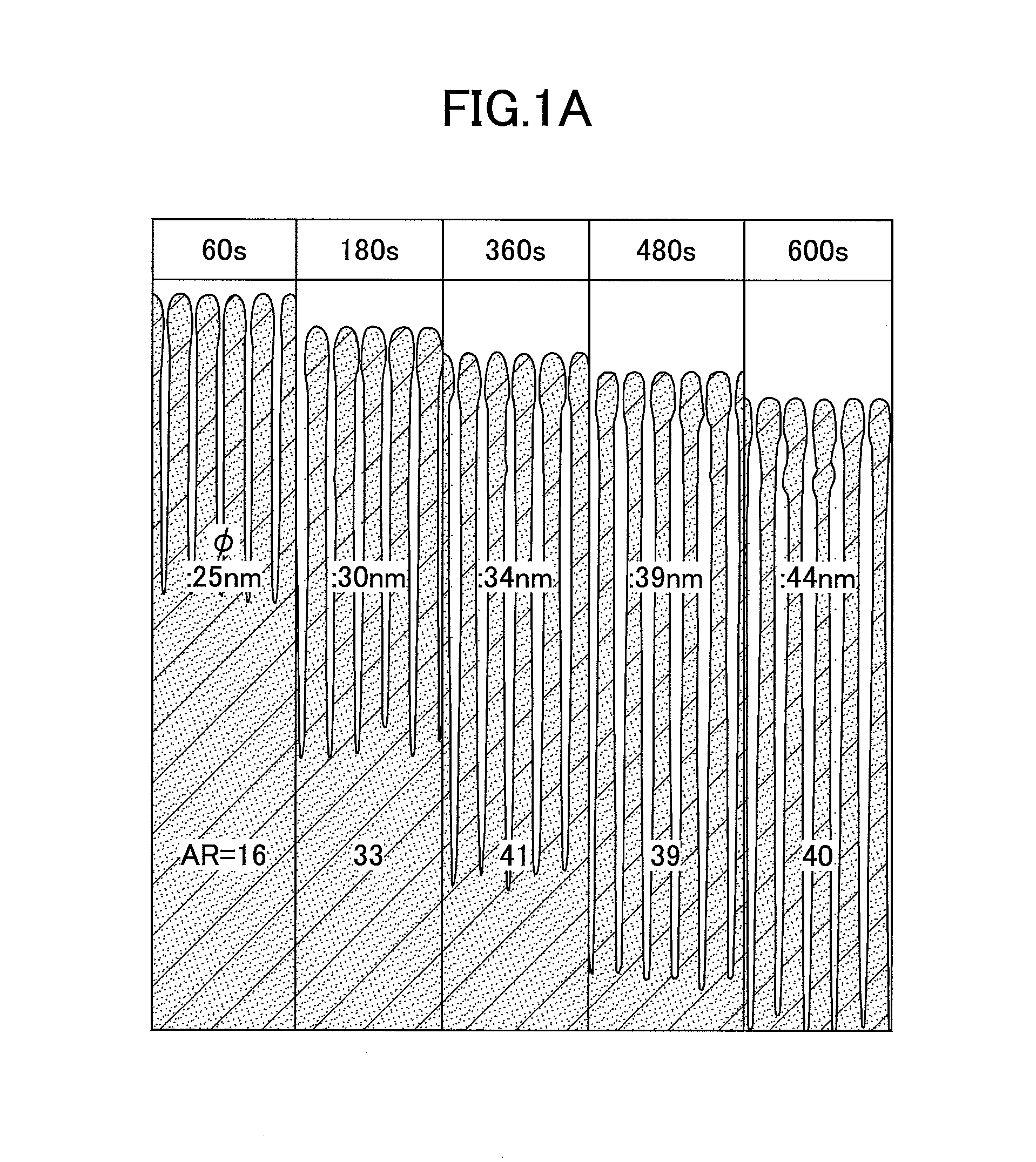
[0037]In the method of forming the pattern according to the first embodiment, as illustrated in “(a) INITIAL STATE” of FIG. 3, a process of forming a pattern illustrated in FIG. 4 is performed in an initial state in which the silicon oxide film (SiO2) 26, the silicon nitride film (SiN) 27 and a poly-silicon mask 28 are sequentially deposited on a silicon substrate (Si) 25 from the bottom. FIG. 4 is a flowchart illustrating the method of forming the pattern according to the first embodiment. Here, a hole pattern having a diameter of 25 nm is formed in the poly-silicon mask 28 by using photolithography technology.

[0038][Process of Forming Pattern]

[0039](Etching Process)

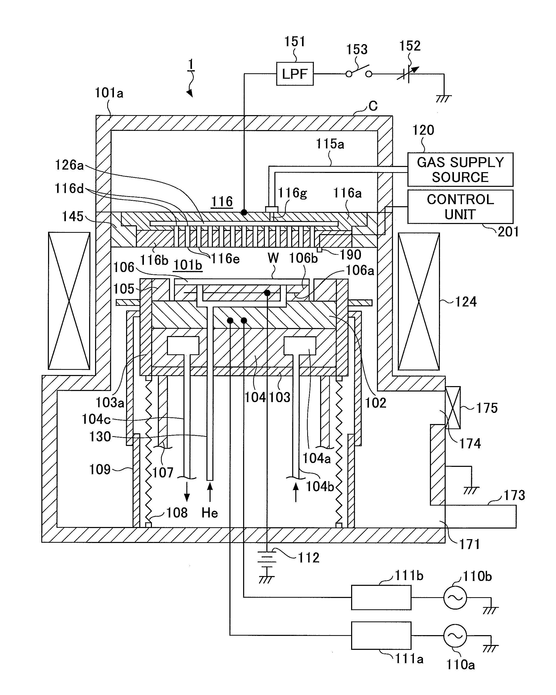
[0040]After starting the process of forming the pattern illustrated in FIG. 4, an etching process is performed in step S10. In this experiment, a lower two-frequency application type parallel flat plate etching apparatus (see FIG. 10) is used among parallel flat plate plasma processing apparatuses. Process conditions of...

second embodiment

[0086]Next, a description is given below of a method of forming a pattern according to a second embodiment with reference to FIG. 8. FIG. 8 is a flowchart illustrating a process of forming a pattern according to the second embodiment. In the process of forming the pattern according to the second embodiment, a process of calculating a repeat count of the ALD process in steps S30 and S32 is performed in addition to steps S10, S12 and S14 of the process of forming the pattern according to the first embodiment illustrated in FIG. 4.

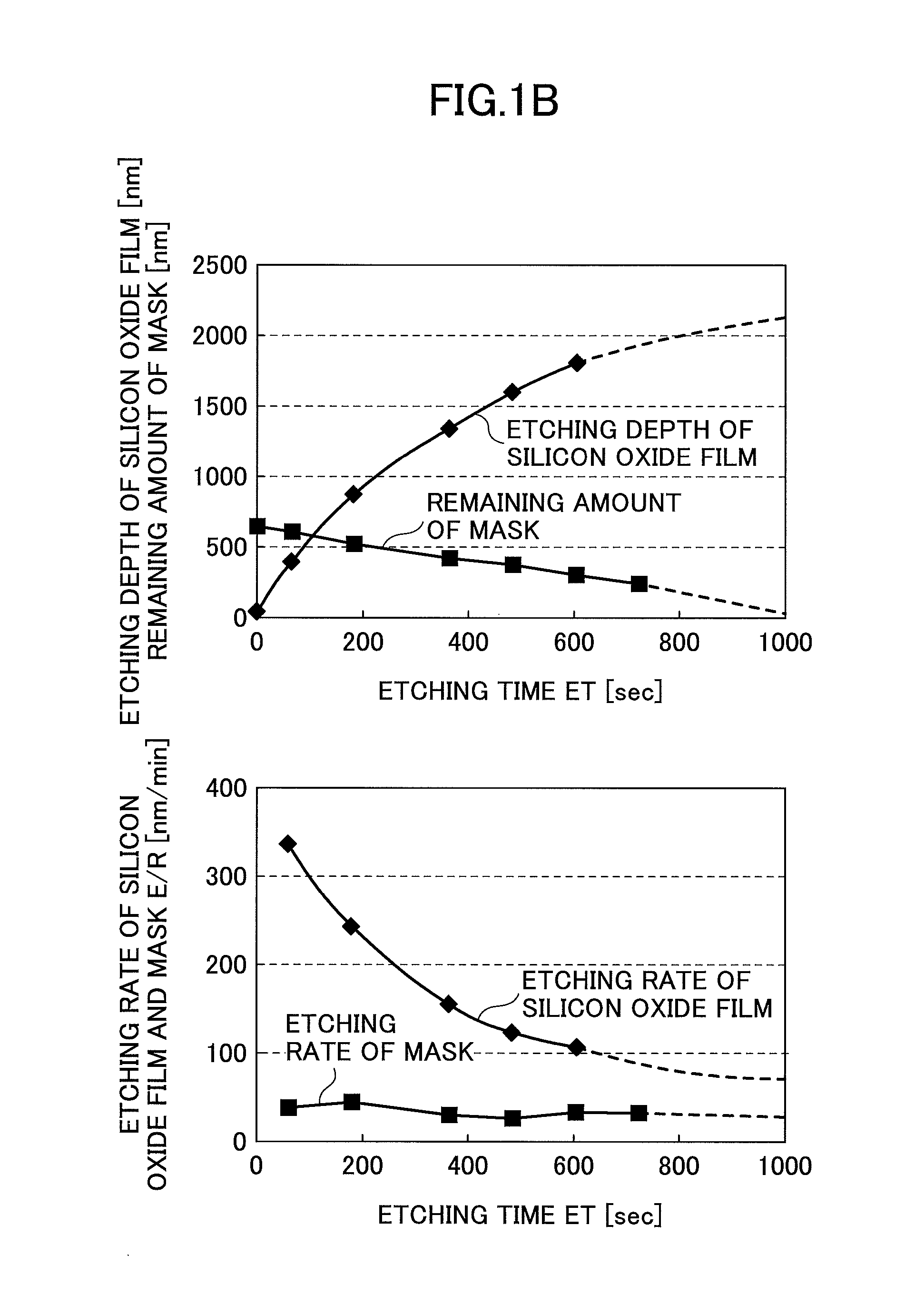
[0087]In other words, in the process of forming the pattern according to the second embodiment, at step S30, a shape of an etched hole is monitored while or after performing the etching process of step S10. In step S32, a diameter of the etched hole is calculated based on the result of the monitor; a film thickness to be deposited on a surface of the hole is calculated depending on the calculated diameter of the hole; and the repeat count n of the ALD process...


PUM

PropertyMeasurementUnit
aspect ratioaaaaaaaaaa
diameteraaaaaaaaaa
diameteraaaaaaaaaa

Abstract

A method of forming a pattern is provided. The method includes an etching step of forming a predetermined pattern in a silicon-containing film by etching the silicon-containing film deposited on a substrate through a mask by plasma generated from an etching gas containing a fluorocarbon gas, and a film deposition step of depositing a silicon oxide film or a silicon nitride film on a surface of the predetermined pattern by oxidizing or nitriding a silicon-containing layer adsorbed on the surface of the predetermined pattern by supplying a silicon compound gas, by using plasma generated from an oxidation gas or a nitriding gas.

Description

CROSS-REFERENCE TO RELATED APPLICATIONS[0001]The present application is a National Stage of International Application No. PCT / JP2013 / 068883 filed on Jul. 10, 2013, claiming priority based on Japanese Patent Application No. 2012-155359 filed on Jul. 11, 2012, and U.S. Provisional Application No. 61 / 672,399 filed on Jul. 17, 2012, the entire contents of which are hereby incorporated by reference.TECHNICAL FIELD[0002]The present invention relates to a method of forming a pattern and a substrate processing system.BACKGROUND ART[0003]When forming a deep hole (a contact hole) having a high aspect ratio by plasma etching, an amount of radicals reaching a bottom of the hole decreases as the bottom of the hole becomes deeper, and an etching rate decreases.[0004]When the etching rate decreases in a depth direction as the bottom of the hole becomes deeper, a bowing shape is formed in the hole that has a hole diameter larger in a lower position than in an upper position (see [b] in FIG. 2). Mor...

Claims


Application Information

Patent Timeline
Patent Type & Authority Patents(United States)
IPC IPC(8): C23F1/02C23C16/34H01L21/67H01L21/02H01L21/311H01J37/32H01L21/768C23C16/04C23C16/455C23C16/40
CPCH01L21/31116H01L21/31144H01L21/67069H01L21/76816C23C16/45525C23C16/045C23C16/345C23C16/402C23C16/45542H01J37/32935H01L21/0217H01L21/0228H01L21/02164H01L21/02211H01L21/02219H01L21/02274H01J2237/3347
Inventor KUBOTA, KAZUHIROSHIMIZU, RYUKICHI
Owner TOKYO ELECTRON LTD
Why Eureka
Try Eureka