
Method for forming electrically conductive ultrafine pattern, electrically conductive ultrafine pattern, and electric circuit

a technology of ultrafine patterns and ultrafine patterns, applied in the direction of conductive pattern formation, printed circuit aspects, printed circuit manufacturing, etc., can solve the problems of increased material cost, insufficient productivity, and large equipment investment for large-scale facilities, and achieves convenient acquisition, high productivity, and preferable pattern cross-sectional shape and fineness.

Active Publication Date: 2016-01-07
DAINIPPON INK & CHEM INC
View PDF6 Cites 2 Cited by
  • Summary
  • Abstract
  • Description
  • Claims
  • Application Information

AI Technical Summary

Benefits of technology

The invention is a method that can create very fine and patterned metal traces using reverse offset printing and plating. This method is faster and more efficient than traditional methods like photolithography, and can easily create complex patterns. The resulting metal traces are electrically conductive, making them useful in a variety of applications.

Problems solved by technology

However, in a photolithographic method, steps including metal deposition, resist coating, exposure using a mask, unnecessary resist removal, metal etching, and remaining resist removal are required, and as a result, there have been many problems as described below.
For example, a huge equipment investment for large scale facilities is required, and the productivity is not sufficient due to complicated production steps.
Furthermore, since the procedure is performed in such a way that after a metal film is once formed on the entire surface, unnecessary portions of the film are then removed, a material cost is increased, and environmental load is also high.
In recent years, in order to overcome the problems of the equipment cost, the material cost, and the productivity of a photolithographic method, the formation of an electrically conductive ultrafine pattern has been attempted by a printing method; however, for example, the electrical conductivity of an electrically conductive pattern formed by a printing method is disadvantageously inferior to that formed by a photolithographic method, and as a result, a practically usable electrically conductive pattern has not been developed yet.
In addition, in order to overcome the problems of the equipment cost, the material cost, and the productivity of a photolithographic method, and the problem of a low electrical conductivity of a printing method, a fusion technique of a printing process and a plating process (such as a technique of forming an electrically conductive pattern in which after an electrically conductive ink containing an electrically conductive substance, such as silver, or a plating core agent is applied on a surface of a support member and then fired to form a plating core pattern, the surface thereof is processed by a plating treatment to form a plating layer on the surface of the plating core pattern) has drawn attention (for example, see PTLs 1, 2, and 3).
In addition, as a laminate including a plating core pattern, although a laminate having excellent adhesion at the respective interfaces among an object on which printing is to be performed, the plating core pattern, and the plating core pattern is desired, a laminate capable of satisfying all of them has not been found yet.

Method used


Image

  • Method for forming electrically conductive ultrafine pattern, electrically conductive ultrafine pattern, and electric circuit
  • Method for forming electrically conductive ultrafine pattern, electrically conductive ultrafine pattern, and electric circuit

Examples


synthetic example 1

Synthesis of Urethane Resin (a1-1)>

[0224]In a nitrogen-purged container equipped with a thermometer, a nitrogen gas inlet tube, and a stirrer, 100 parts by mass of a polyester polyol (polyester polyol obtained by a reaction among 1,4-cyclohexanedimethanol, neopentyl glycol, and adipic acid, hydroxyl equivalent: 1,000 g / equivalent), 17.4 parts by mass of 2,2-dimethylolpropionic acid, 21.7 parts by mass of 1,4-cyclohexanedimethanol, and 106.2 parts by mass of dicyclohexylmethanediisocyanate were mixed in 178 parts by mass of methyl ethyl ketone and were allowed to react with each other, so that an organic solvent solution of a urethane prepolymer having an isocyanate group at the terminal was obtained. Subsequently, 44.7 parts by mass of pentaerythritol triacrylate was mixed with the organic solvent solution of the urethane prepolymer so as to allow the urethane prepolymer to react with pentaerythritol triacrylate, so that an organic solvent solution of a urethane resin having a vinyl...

synthetic example 2

Synthesis of Urethane Resin (a1-2)

[0225]In a nitrogen-purged container equipped with a thermometer, a nitrogen gas inlet tube, and a stirrer, 100 parts by mass of a polyester polyol (polyester polyol obtained by a reaction among 1,4-cyclohexanedimethanol, neopentyl glycol, and adipic acid, hydroxyl equivalent: 1,000 g / equivalent), 17.4 parts by mass of 2,2-dimethylolpropionic acid, 21.7 parts by mass of 1,4-cyclohexanedimethanol, and 106.2 parts by mass of dicyclohexylmethanediisocyanate were mixed in 178 parts by mass of methyl ethyl ketone and were allowed to react with each other, so that an organic solvent solution of a urethane prepolymer having an isocyanate group at the molecular terminal was obtained. Subsequently, the carboxyl group of the urethane resin was partially or entirely neutralized by adding 13.3 parts by mass of triethylamine to the organic solvent solution of the urethane prepolymer, and 277 parts by mass of water was further added thereto and sufficiently stirr...

synthetic example 3

Synthesis of Urethane Resin (a1-3)

[0226]In a nitrogen-purged container equipped with a thermometer, a nitrogen gas inlet tube, and a stirrer, 100 parts by mass of a polyether polyol (hydroxyl equivalent: 1,000 g / equivalent) obtained by adding propylene oxide to bisphenol A, 21.6 parts by mass of 1,4-cyclohexanedimethanol, 66.8 parts by mass of dicyclohexylmethanediisocyanate were mixed in 178 parts by mass of methyl ethyl ketone and were allowed to react with each other, so that an organic solvent solution of a urethane prepolymer having an isocyanate group at the terminal was obtained. Subsequently, 9.6 parts by mass of methyl ethyl ketone oxime was mixed with the organic solvent solution of the urethane prepolymer to allow the urethane prepolymer to react with methyl ethyl ketone oxime, so that an organic solvent solution of a urethane resin (a1-3) having a blocked isocyanate group was obtained.


PUM

PropertyMeasurementUnit
volume average particle diameteraaaaaaaaaa
thicknessaaaaaaaaaa
temperatureaaaaaaaaaa

Abstract

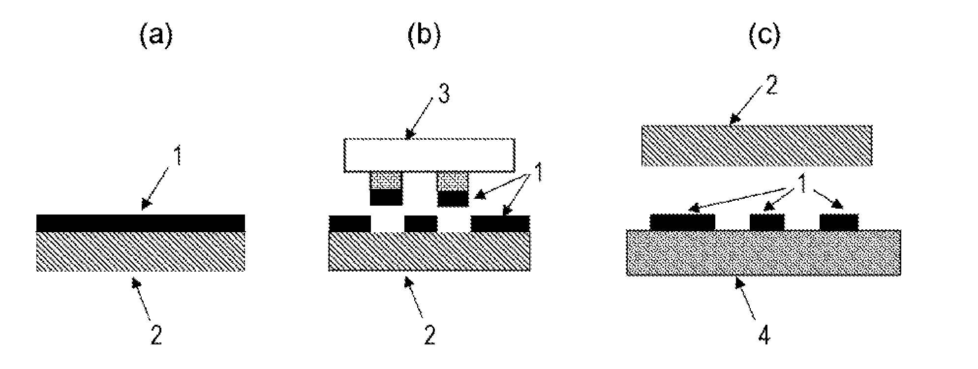
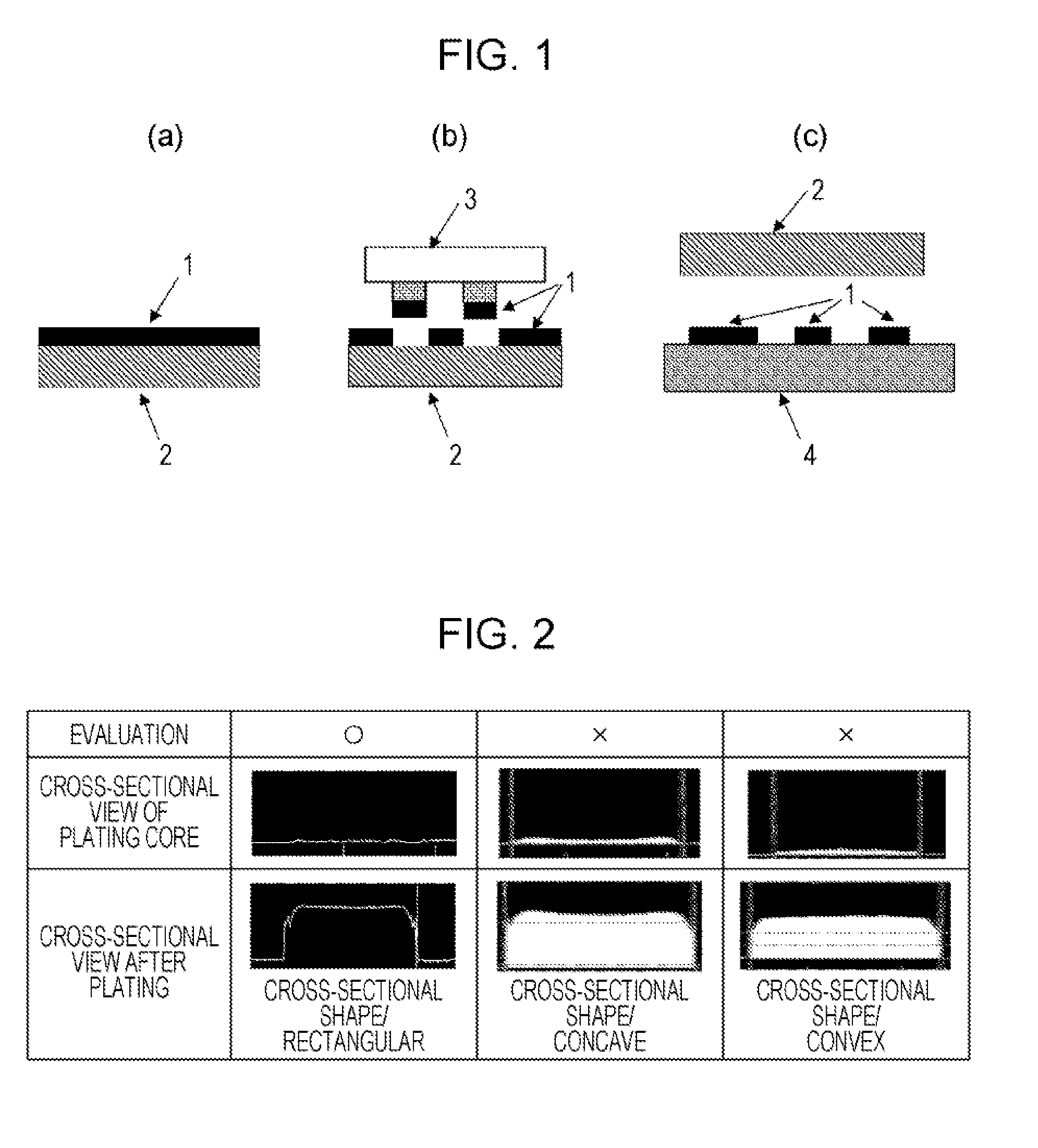
There is provided a method for forming an electrically conductive ultrafine pattern which has an excellent pattern cross-sectional shape is provided by a composite technique including a printing process and a plating process, and furthermore, by imparting excellent adhesion to each interface of a laminate including a plating core pattern, an electrically conductive ultrafine pattern which can be preferably used as a highly accurate electric circuit and a method for manufacturing the same are also provided. The method includes (1) a step of applying a resin composition to form a receiving layer on a substrate; (2) a step of printing an ink containing plating core particles by a reverse offset printing method to form a plating core pattern on the receiving layer; and (3) a step of depositing a metal on the plating core pattern formed in the step (2) by an electrolytic plating method.

Description

TECHNICAL FIELD[0001]The present invention relates to a method for forming an electrically conductive ultrafine pattern, the method including a plating core ink printing process and an electrolytic plating process performed on a plating core pattern; the pattern described above; and an electric circuit including the pattern described above.BACKGROUND ART[0002]Heretofore, for the formation of an electrically conductive ultrafine pattern, in general, a photolithographic method capable of performing ultrafine patterning has been used. However, in a photolithographic method, steps including metal deposition, resist coating, exposure using a mask, unnecessary resist removal, metal etching, and remaining resist removal are required, and as a result, there have been many problems as described below. For example, a huge equipment investment for large scale facilities is required, and the productivity is not sufficient due to complicated production steps. Furthermore, since the procedure is ...

Claims


Application Information

Patent Timeline
Patent Type & Authority Applications(United States)
IPC IPC(8): H05K3/18C25D5/02C25D5/56C25D7/00H05K1/03H05K1/09H05K3/12
CPCH05K3/188C25D5/56C25D5/02C25D7/00H05K2201/09218H05K1/0313H05K3/12H05K2201/0203H05K1/097H05K3/207H05K3/246H05K2203/0108H05K2203/097H05K2201/0224H05K2201/0257
Inventor YOSHIHARA, SUNAOKATSUTA, HARUHIKOKATAYAMA, YOSHINORISHIRAKAMI, JUNMURAKAWA, AKIRAFUJIKAWA, WATARUSAITOU, YUKIE
Owner DAINIPPON INK & CHEM INC
Learn More