

Method for forming electrically conductive ultrafine pattern, electrically conductive ultrafine pattern, and electric circuit
a technology of ultrafine patterns and ultrafine patterns, applied in the direction of conductive pattern formation, printed circuit aspects, printed circuit manufacturing, etc., can solve the problems of increased material cost, insufficient productivity, and large equipment investment for large-scale facilities, and achieves convenient acquisition, high productivity, and preferable pattern cross-sectional shape and fineness.
- Summary
- Abstract
- Description
- Claims
- Application Information
AI Technical Summary
Benefits of technology
Problems solved by technology
Method used
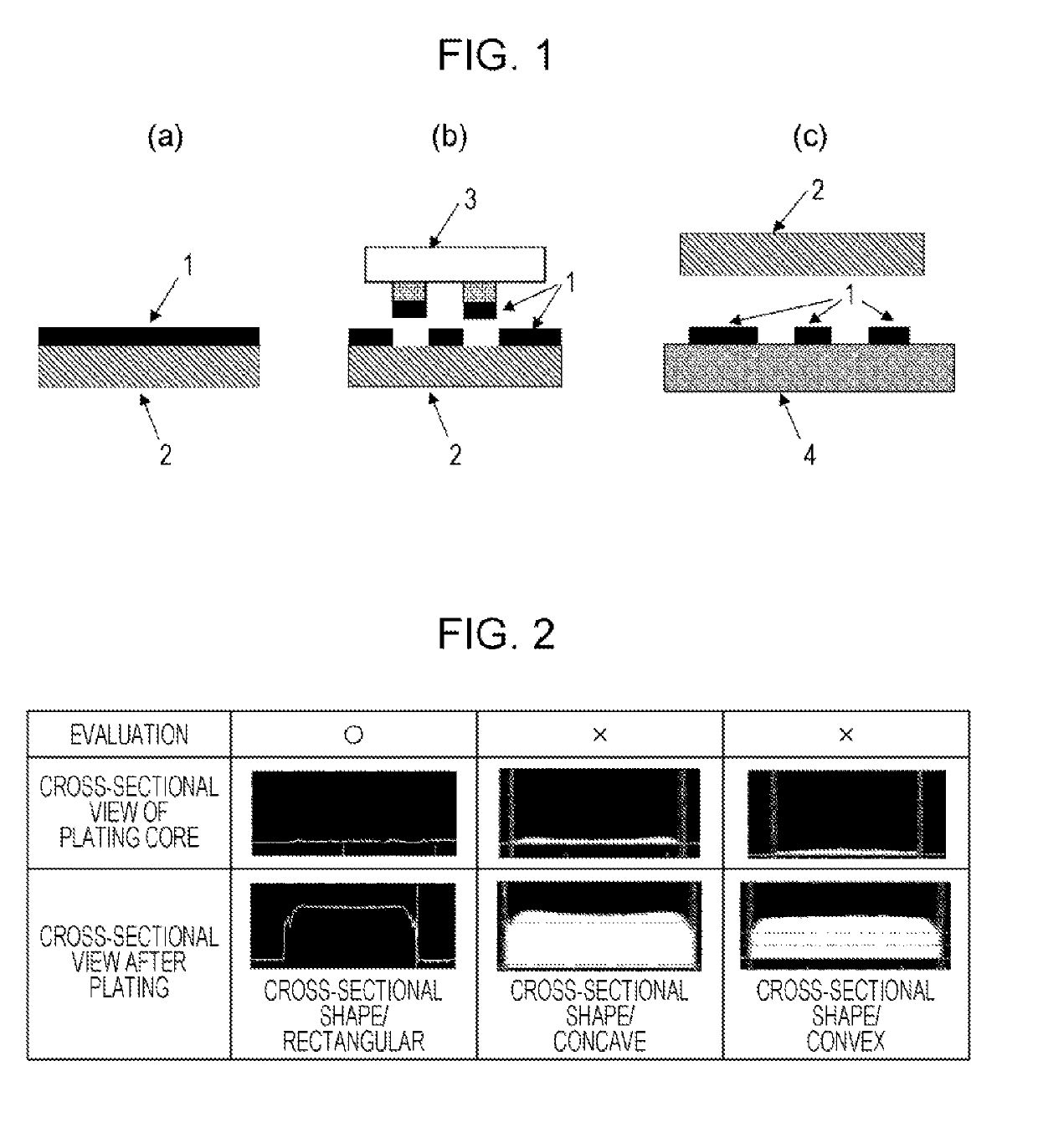
Image

Examples
synthetic example 1
Synthesis of Urethane Resin (a1-1)
[0224]In a nitrogen-purged container equipped with a thermometer, a nitrogen gas inlet tube, and a stirrer, 100 parts by mass of a polyester polyol (polyester polyol obtained by a reaction among 1,4-cyclohexanedimethanol, neopentyl glycol, and adipic acid, hydroxyl equivalent: 1,000 g / equivalent), 17.4 parts by mass of 2,2-dimethylolpropionic acid, 21.7 parts by mass of 1,4-cyclohexanedimethanol, and 106.2 parts by mass of dicyclohexylmethanediisocyanate were mixed in 178 parts by mass of methyl ethyl ketone and were allowed to react with each other, so that an organic solvent solution of a urethane prepolymer having an isocyanate group at the terminal was obtained. Subsequently, 44.7 parts by mass of pentaerythritol triacrylate was mixed with the organic solvent solution of the urethane prepolymer so as to allow the urethane prepolymer to react with pentaerythritol triacrylate, so that an organic solvent solution of a urethane resin having a vinyl ...
synthetic example 2
Synthesis of Urethane Resin (a1-2)
[0225]In a nitrogen-purged container equipped with a thermometer, a nitrogen gas inlet tube, and a stirrer, 100 parts by mass of a polyester polyol (polyester polyol obtained by a reaction among 1,4-cyclohexanedimethanol, neopentyl glycol, and adipic acid, hydroxyl equivalent: 1,000 g / equivalent), 17.4 parts by mass of 2,2-dimethylolpropionic acid, 21.7 parts by mass of 1,4-cyclohexanedimethanol, and 106.2 parts by mass of dicyclohexylmethanediisocyanate were mixed in 178 parts by mass of methyl ethyl ketone and were allowed to react with each other, so that an organic solvent solution of a urethane prepolymer having an isocyanate group at the molecular terminal was obtained. Subsequently, the carboxyl group of the urethane resin was partially or entirely neutralized by adding 13.3 parts by mass of triethylamine to the organic solvent solution of the urethane prepolymer, and 277 parts by mass of water was further added thereto and sufficiently stirr...
synthetic example 3
Synthesis of Urethane Resin (a1-3)
[0226]In a nitrogen-purged container equipped with a thermometer, a nitrogen gas inlet tube, and a stirrer, 100 parts by mass of a polyether polyol (hydroxyl equivalent: 1,000 g / equivalent) obtained by adding propylene oxide to bisphenol A, 21.6 parts by mass of 1,4-cyclohexanedimethanol, 66.8 parts by mass of dicyclohexylmethanediisocyanate were mixed in 178 parts by mass of methyl ethyl ketone and were allowed to react with each other, so that an organic solvent solution of a urethane prepolymer having an isocyanate group at the terminal was obtained. Subsequently, 9.6 parts by mass of methyl ethyl ketone oxime was mixed with the organic solvent solution of the urethane prepolymer to allow the urethane prepolymer to react with methyl ethyl ketone oxime, so that an organic solvent solution of a urethane resin (a1-3) having a blocked isocyanate group was obtained.
PUM
| Property | Measurement | Unit |
|---|---|---|
| volume average particle diameter | aaaaa | aaaaa |
| thickness | aaaaa | aaaaa |
| temperature | aaaaa | aaaaa |
Abstract
Description
Claims
Application Information