Solid-state imaging device and method for manufacturing the same

a solid-state imaging and imaging device technology, applied in the direction of solid-state devices, transistors, radiation controlled devices, etc., can solve the problems of adverse smear phenomenon, ineffective reduction of smear components on the surface of substrates, and inability to effectively prevent smear, so as to prevent color mixing phenomenon, effective prevention of signal leakage between adjacent photosensors and between photosensors and transfer sections, and effective prevention of color mixing phenomenon

Active Publication Date: 2005-02-17
SONY CORP
View PDF9 Cites 26 Cited by
  • Summary
  • Abstract
  • Description
  • Claims
  • Application Information

AI Technical Summary

Benefits of technology

[0025] Therefore, the leakage of signal charges between adjacent photosensors and between a photosensor and a transfer section can be effectively prevented; thus, a color mixing phenomenon can be effectively prevented.
[0026] Since multiple times of ion implantation are made for multiple implantation areas during multiple times of impurity ion implanting processes, the dispersion of impurity particularly deep in the substrate can be prevented, effects to a photoelectric conversion section can be reduced, and decreases in sensitivity and saturation signals can be effectively prevented.
[0027] Since the multiple times of ion implantation are made at multiple ion concentrations during multiple times of impurity ion implanting processes, the impurity regions of the respective layers of the channel stop section can be given optimum impurity concentration; thus, anti-smear measures on the surface of the substrate can be effectively taken.
[0028] Since a solid-state imaging device according to the invention includes a channel stop section having multiple layers across the depth of the substrate, the leakage of signal charges between adjacent photosensors and between a photosensor and a transfer section can be effectively prevented; thus, a color mixing phenomenon can be effectively prevented.
[0029] Since the areas of the multiple layers of the channel stop section are multiple, the dispersion of impurity particularly deep in the substrate can be prevented, effects to a photoelectric conversion section can be reduced, and decreases in sensitivity and saturation signals can be effectively prevented.
[0030] Furthermore, since the ion concentrations of the multiple layers of the channel stop section are optimum, anti-smear measures on the surface of the substrate can be effectively taken.

Problems solved by technology

Therefore, the structure of the related-art channel stop section that is formed only in the outer layer of the substrate has the problem of not effectively preventing a phenomenon in which electric charges that are photoelectrically converted in the photodiode region are mixed to the adjacent photosensors (hereinafter, referred to as a color mixing phenomenon).
However, when ions are implanted with high energy, the P-type impurity near the surface declines in concentration and so a smear component in the surface of the substrate cannot be reduced, leading an adverse smear phenomenon.
The ion plantation with high energy has the problem of easily causing dispersion of the P-type impurity, narrowing a charge storage region of the light receiving section (photodiode region), which decreases sensitivity and saturation signals.

Method used


Image

  • Solid-state imaging device and method for manufacturing the same
  • Solid-state imaging device and method for manufacturing the same
  • Solid-state imaging device and method for manufacturing the same

Examples


Embodiment Construction

[0039] Embodiments of a solid-state imaging device and a method for manufacturing the same according to the present invention will be specifically described hereinafter.

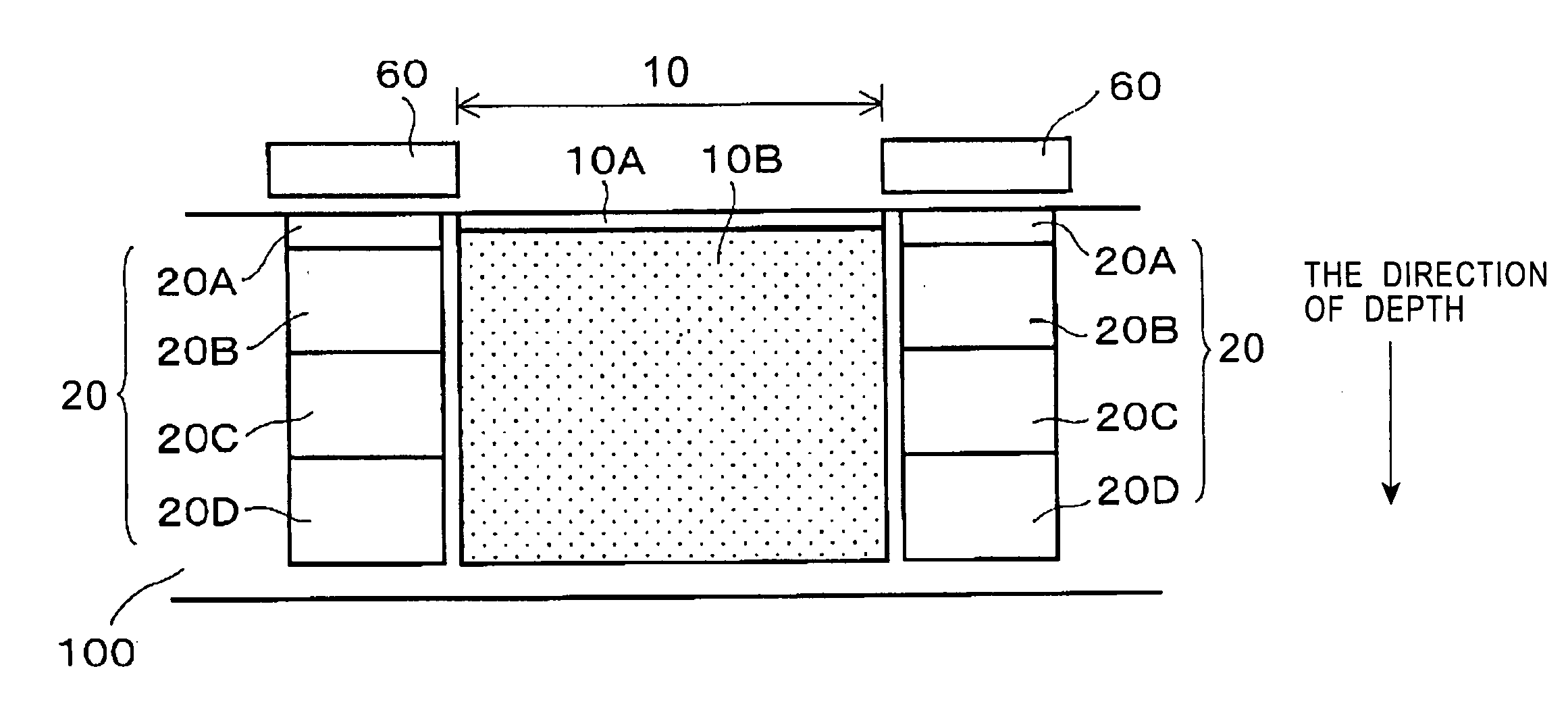
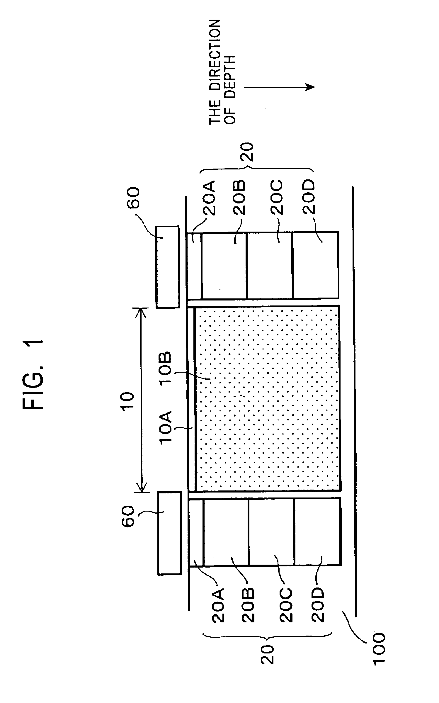
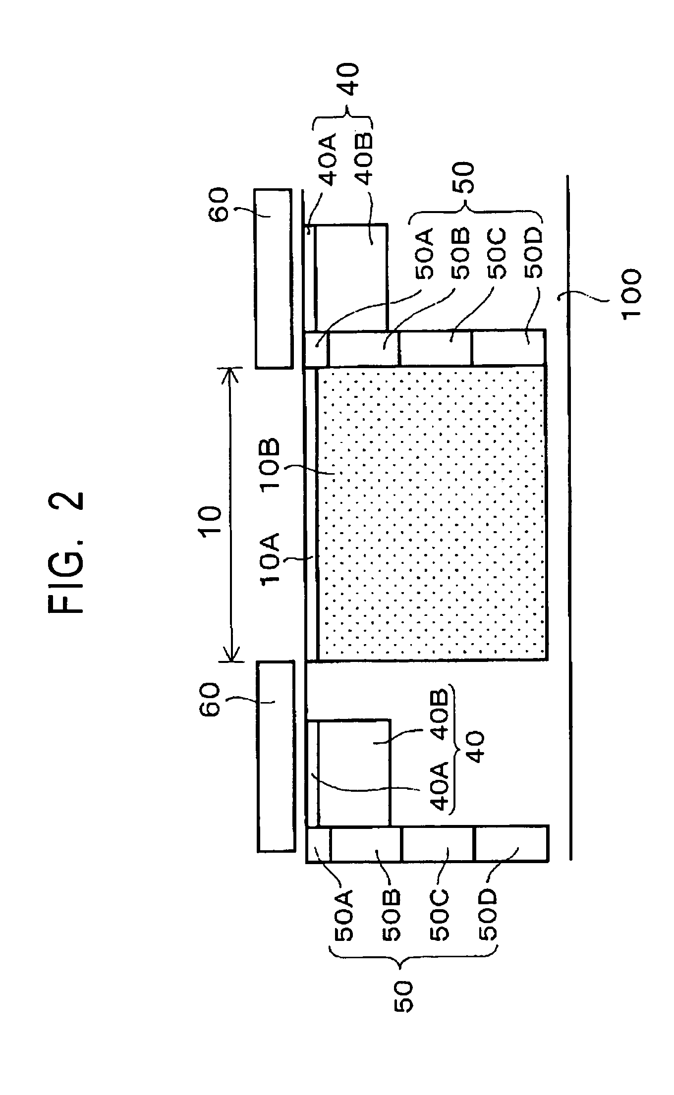
[0040]FIGS. 1 and 2 are sectional views of a solid-state imaging device manufactured by the method according to an embodiment, FIG. 1 showing an embodiment of a channel stop section provided between photosensors along the vertical transfer direction, and FIG. 2 showing an embodiment of a channel stop section provided between the photosensors along the horizontal transfer direction. The entire structure of the solid-state imaging device is the same as that of the related art shown in FIG. 6, wherein FIG. 1 corresponds to the section taken along line A-A of FIG. 6 and FIG. 2 corresponds to the section taken along line B-B of FIG. 6.

[0041] Referring first to FIG. 1, a photodiode region constituting a light receiving section 10 of each photosensor includes a P+ type impurity region (hole storage region) 10A formed in t...


PUM


Abstract

Channel stop sections are formed by multiple times of impurity ion implanting processes. Four-layer impurity regions are formed across the depth of a semiconductor substrate (across the depth of the bulk), so that a P-type impurity region is formed deep in the semiconductor substrate; thus, incorrect movement of electric charges is prevented. Other four-layer impurity regions of another channel stop section are decreased in width step by step across the depth of the substrate, so that the reduction of a charge storage region of a light receiving section due to the dispersion of P-type impurity in the channel stop section is prevented in the depth of the substrate.

Description

BACKGROUND OF THE INVENTION [0001] 1. Field of the Invention [0002] The present invention relates to a solid-state imaging device formed by integrating a plurality of photosensors on a substrate in which a channel stop section for preventing leakage of electric charges between the photosensors can be effectively formed and to a method for manufacturing the same. [0003] 2. Description of the Related Art [0004]FIG. 6 is an explanatory view of an example of the arrangement of a CCD solid-state imaging device. [0005] The solid-state imaging device includes a photosensor (imaging region) 410, a CCD vertical transfer section 420, a CCD horizontal transfer section 430, an output 440 and so on in a substrate 400. [0006] The photosensor 410 has a plurality of the CCD vertical transfer sections 420 along the respective photosensor trains, in which signal charges stored by the photosensors 412 are output to the CCD vertical transfer sections 420 and sequentially transferred in the vertical dir...

Claims


Application Information

Patent Timeline
Patent Type & Authority Applications(United States)
IPC IPC(8): H01L27/148H01L27/146H01L29/768
CPCH01L27/1463H01L27/14656H01L27/14689H01L27/14806H01L27/1461H01L27/14831H01L27/14887H01L31/035272H01L27/14812H01L27/14612H01L27/14616H01L27/14643H01L27/148
Inventor HIRATA, KIYOSHI
Owner SONY CORP
Why Eureka
Try Eureka