Liquid crystal display and panel therefor

a technology of liquid crystal display and thin film transistor, which is applied in the direction of instruments, semiconductor devices, optics, etc., can solve the problems of inability to perceive images, poor lateral visibility, and disappearance of luminance difference between high grays, so as to improve picture quality

Active Publication Date: 2005-02-17
SAMSUNG DISPLAY CO LTD
View PDF3 Cites 228 Cited by
  • Summary
  • Abstract
  • Description
  • Claims
  • Application Information

AI Technical Summary

Benefits of technology

[0010] The invention is directed to a flat panel display having an improved picture quality. In one embodiment the flat panel display includes a common electrode formed of a transparent conductive material and having at least one cutout therein. One or more pixel areas are positioned under the common electrode, and each pixel area includes one or more subpixel areas. A liquid crystal (LC) layer is disposed between the common electrode and the one or more subpixel areas, and the LC layer includes a plurality of LC molecules.
[0011] In each subpixel area, a first pixel electrode and a second pixel electrode are formed that engage with each other and enclose an open space (gap) such that their outer boundary has a substantially rectangular shape. The first pixel electrode includes a pair of right-angled triangular shaped portions facing one or more oblique edges of the second pixel electrode and also includes a longitudinal portion facing a side edge of the second pixel electrode. The second pixel electrode has a shape that approximates an equilateral trapezoid. The second electrode may also have an edge thereof disposed proximate a first storage electrode and another edge disposed proximate a second storage electrode. The gap formed between the first and second electrodes is disposed between the at least one cutout formed in the common electrode and an opening that separates a pixel area from another of the one or more pixel areas.
[0012] The flat panel display may also include a capacitance electrode coupled to the second pixel electrode to form a coupling capacitor. In use, the coupling capacitor operates such that a magnitude of a voltage applied to the first pixel electrode is lower than an applied data voltage, and a magnitude of a voltage applied to the second pixel electrode is higher than an applied voltage. The different voltages operate such that a tilt direction of LC molecules disposed above the first pixel electrode differs from a-tilt direction of LC molecules disposed above the second pixel electrode.

Problems solved by technology

For example, the quality of lateral visibility is poor as compared with front visibility.
In serious cases, the luminance difference between high grays vanishes such that the images cannot be perceived.
Additionally, VA mode LCDs often have poor response times. For example, although the LC molecules near the cutouts or protrusions rapidly tilt in a direction in response to a strong fringe field, the LC molecules far from the cutouts or protrusions may experience a weak fringe field and may not rapidly determine the tilt directions.
Narrowing the distance between the cutouts may improve response times, but it may also reduce the aperture ratio.

Method used


Image

  • Liquid crystal display and panel therefor
  • Liquid crystal display and panel therefor
  • Liquid crystal display and panel therefor

Examples


Embodiment Construction

[0031] The present invention is described more fully hereinafter with reference to the accompanying drawings, in which preferred embodiments of the invention are shown. The present invention may, however, be embodied in many different forms and should not be construed as limited to the embodiments set forth herein.

[0032] In the drawings, the thickness of layers, films and regions are exaggerated for clarity. Like numerals refer to like elements throughout. It will be understood that when an element such as a layer, film, region or substrate is referred to as being “on” another element, it can be directly on the other element or intervening elements may also be present. In contrast, when an element is referred to as being “directly on” another element, there are no intervening elements present.

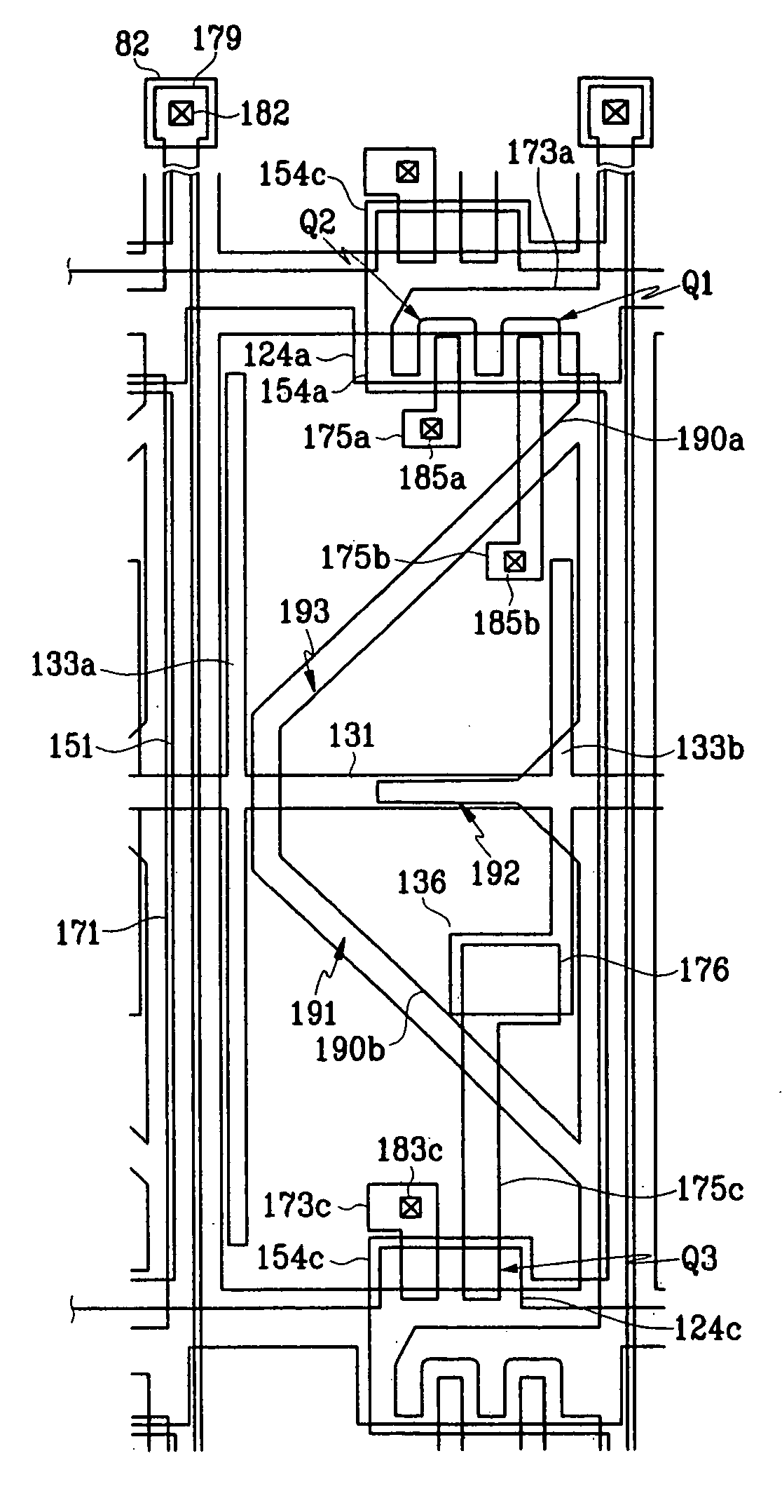
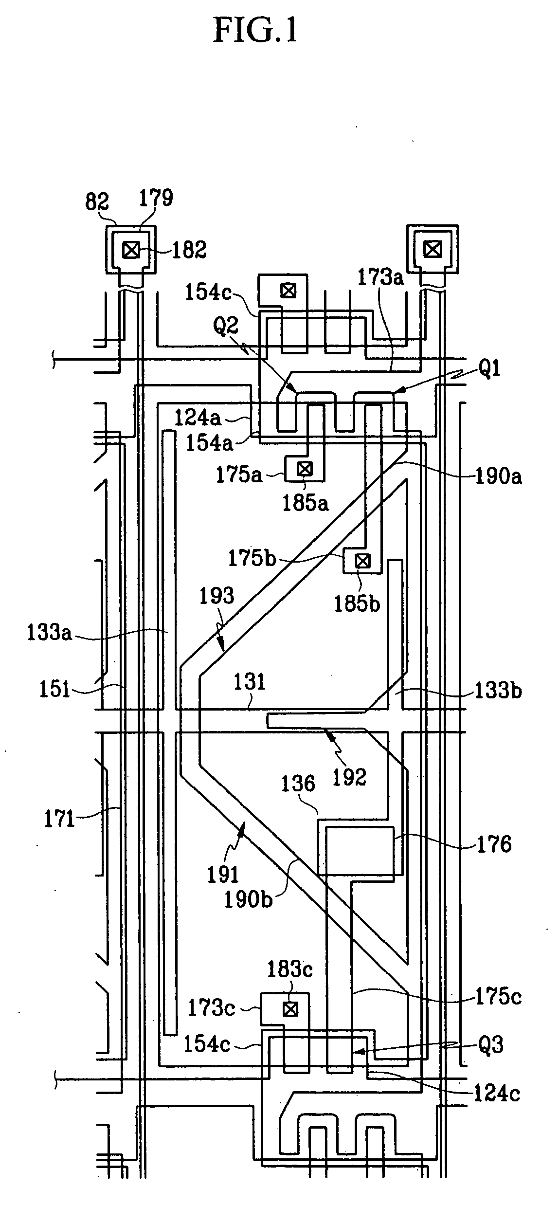
[0033] A LCD according to an embodiment of the present invention is described in detail with reference to FIGS. 1-6. FIG. 1 is a top view of a TFT array panel of a LCD according to an embodim...


PUM

PropertyMeasurementUnit
widthaaaaaaaaaa
voltageaaaaaaaaaa
voltageaaaaaaaaaa

Abstract

A flat panel display having an improved picture quality is disclosed. In one embodiment, a first pixel electrode and a second pixel electrode are formed in each subpixel area. The electrodes enclose an open space (gap) such that their outer boundary has a substantially rectangular shape. The flat panel display may also include a capacitance electrode coupled to the second pixel electrode to form a coupling capacitor. In use, the coupling capacitor operates such that a magnitude of a voltage applied to the first pixel electrode is lower than an applied data voltage, and a magnitude of a voltage applied to the second pixel electrode is higher than an applied voltage. The different voltages operate such that a tilt direction of LC molecules disposed above the first pixel electrode differs from a tilt direction of LC molecules disposed above the second pixel electrode.

Description

CROSS REFERENCE TO RELATED APPLICATIONS [0001] This application claims priority of Korean Application 2003-0056067 filed on Aug. 13, 2003 and to Korean Application 2003-0056546 filed on Aug. 14, 2003. BACKGROUND OF THE INVENTION [0002] 1. Field of the Invention [0003] The present invention relates to liquid crystal displays generally, and more particularly, to an improved thin film transistor (TFT) panel therefor. [0004] 2. Description of Related Art [0005] A liquid crystal display (LCD) is one of the most widely used flat panel displays. A LCD includes two panels provided with field-generating electrodes such as pixel electrodes and a common electrode and a liquid crystal (LC) layer interposed therebetween. The LCD displays images by applying voltages to the field-generating electrodes to generate an electric field in the LC layer, which determines orientations of LC molecules in the LC layer to adjust polarization of incident light. [0006] An example of a LCD is a vertical alignme...

Claims


Application Information

Patent Timeline
Patent Type & Authority Applications(United States)
IPC IPC(8): G02F1/1333G02F1/1343G02F1/1368H01L29/786
CPCG02F1/133707G02F1/1368G02F1/134336G02F1/13624G02F1/134309G02F1/136213G02F1/136286G02F2201/123H01L27/124
Inventor SONG, JANG-KUN
Owner SAMSUNG DISPLAY CO LTD
Why Eureka
Try Eureka