Semiconductor memory device with magnetoresistance elements and method of writing data into the same

a magnetic resistance element and memory device technology, applied in semiconductor devices, digital storage, instruments, etc., can solve the problem of increasing the chip size of the conventional mram, and achieve the effect of increasing the chip siz

Inactive Publication Date: 2005-02-17
KK TOSHIBA
View PDF3 Cites 100 Cited by
  • Summary
  • Abstract
  • Description
  • Claims
  • Application Information

AI Technical Summary

Problems solved by technology

The conventional MRAM, however, has the problem of getting larger in chip size.

Method used


Image

  • Semiconductor memory device with magnetoresistance elements and method of writing data into the same
  • Semiconductor memory device with magnetoresistance elements and method of writing data into the same
  • Semiconductor memory device with magnetoresistance elements and method of writing data into the same

Examples


first embodiment

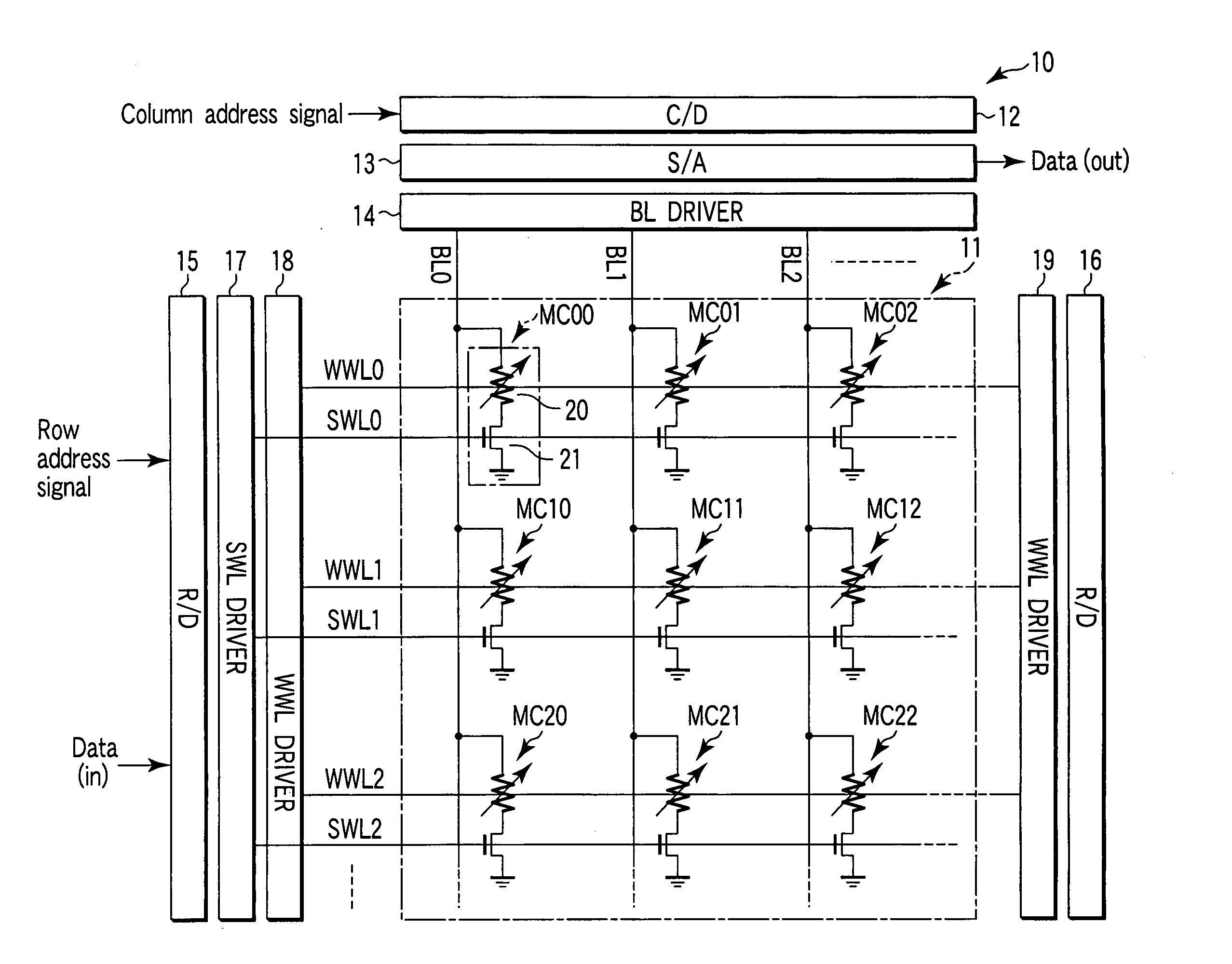
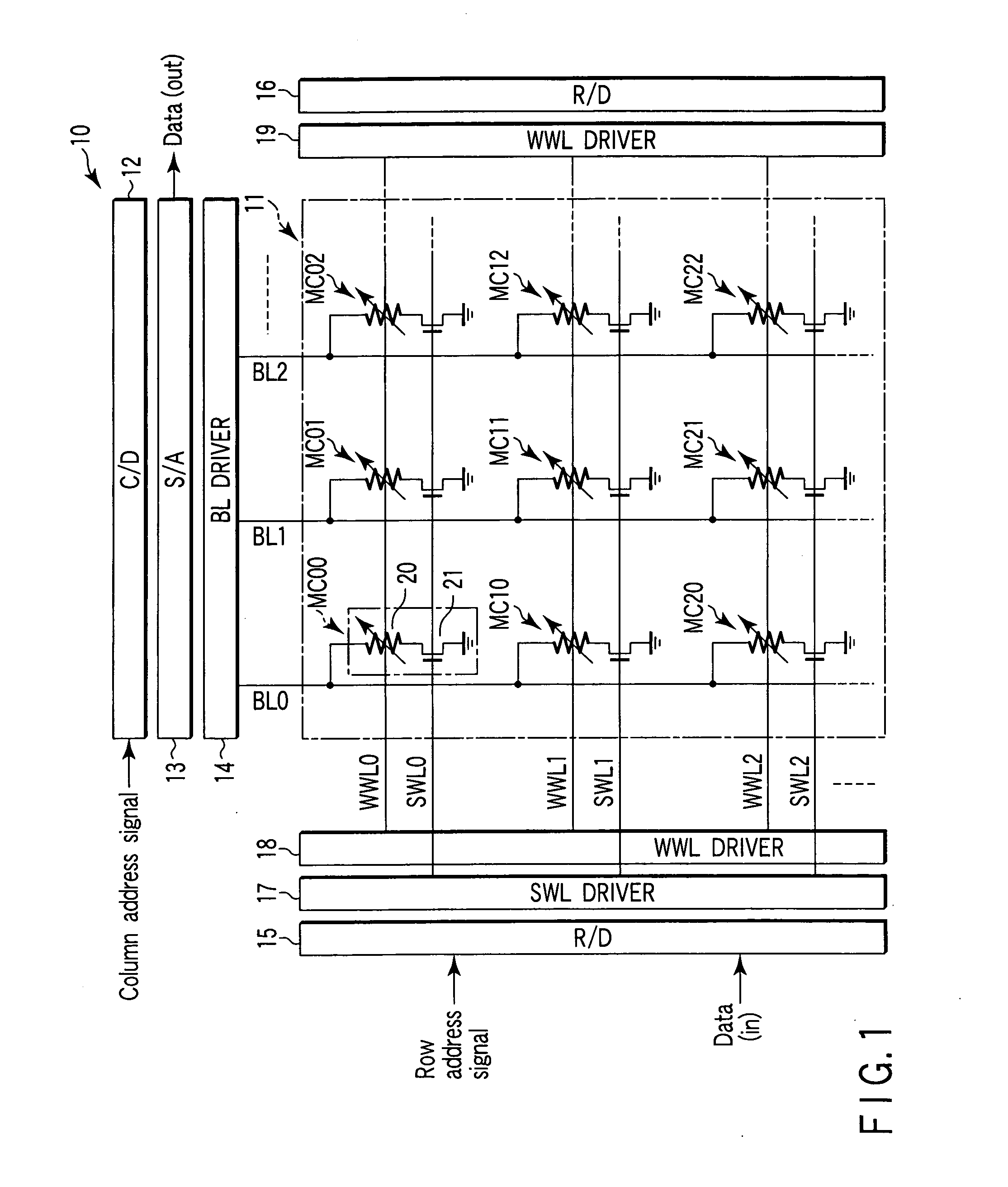
[0099] Next, the operation of the MRAM configured as described above will be explained by reference to FIGS. 1 and 4. A write operation will be explained using a case where data is written into memory cell MC11 provided at the intersection of bit line BL1 and select word line SWL1 (write word line WWL1). FIG. 4 is a flowchart for a write operation in the MRAM of the

[0100] First, the select word line driver 17 selects select word line SWL1 on the basis of a row address decode signal. Then, the select word line driver 17 supplies a voltage to select word line SWL1. This brings the switching transistors 21 of the memory cells MC10, MC11, MC12, . . . , MC1n into the on state (step S1).

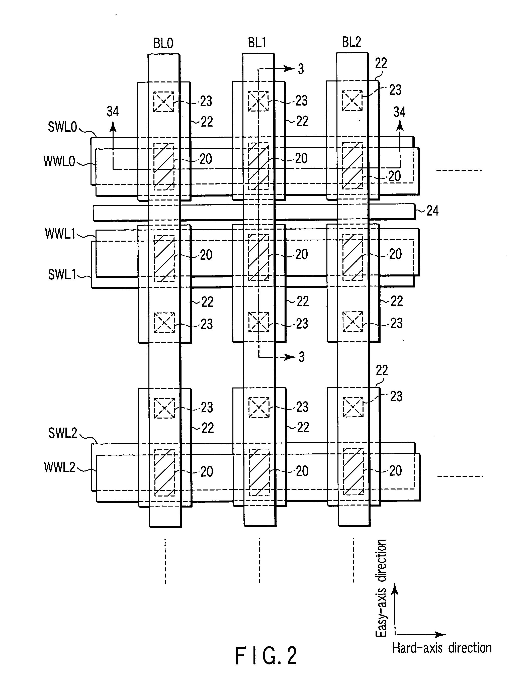
[0101] Next, the bit line driver 14 selects bit line BL1 on the basis of a column address decode signal. Then, the bit line driver 14 supplies a current Iselect of about 10 μA to bit line BL1 (step S2). This is shown in FIG. 5. FIG. 5 is a circuit diagram of a part of the memory cell array 11.

[0102] As s...

second embodiment

[0154] With the data writing method after a write select word line is selected, current is caused to flow in the write word line, with tunnel current flowing in the bit line connected to the memory cell into which “0” data is to be written, thereby writing “0” data. Then, with tunnel current flowing in the bit line connected to the memory cell into which “1” data is to be written, opposite current is caused to flow in the write word line, thereby writing “1” data. By the series of processes, the data has been written into all of the memory cells connected to the same write select word line.

[0155] Moreover, in a read operation, the data held in plurality (all) of the memory cells connected to the same select word line can be read simultaneously by causing current to flow in a plurality of (all) bit lines.

[0156] Accordingly, a plurality of data items can be processed at a time, which enables a high-speed operation. Moreover, when image data or the like is handled, it is desirable th...

third embodiment

[0169] Next, the operation of the MRAM configured as described above will be explained by reference to FIGS. 17 and 20. A write operation will be explained using a case where data is written into memory cell MC11 provided at the intersection of bit line BL1 and select word line SWL1 (write word line WWL1). FIG. 20 is a-flowchart for a write operation in the MRAM of the

[0170] First, in step S31 of FIG. 20, current Iselect is caused to flow from bit line BL1 connected to select memory cell MC11 to select word line SWL1 via the tunnel junction of the magneto-resistive element 20. Specifically, the select word line driver 17 selects select word line SWL1 on the basis of a row address decode signal. At this time, the select word line driver 17 functions as a current sink. Next, the bit line driver 14 selects bit line BL1 on the basis of a column address decode signal. Then, the bit line driver 14 supplies a current Iselect of about 100 μA to bit line BL1. This is shown in FIG. 21. FIG. 2...


PUM


Abstract

A semiconductor memory device includes memory cells, first wirings, a first current driver circuit, and a second current driver circuit. The memory cell includes a magneto-resistive element having a first ferromagnetic film, an insulating film formed on the first ferromagnetic film, and a second ferromagnetic film formed on the insulating film. The first wiring is provided in close proximity to and insulated from the magneto-resistive element. The first current driver circuit supplies a first current to the first wiring in a write operation to produce a magnetic field around the magneto-resistive elements. The second current driver circuit supplies a second current between the first and second ferromagnetic films via the insulating film in a write and a read operation.

Description

CROSS-REFERENCE TO RELATED APPLICATIONS [0001] This application is based upon and claims the benefit of priority from the prior Japanese Patent Application No. 2003-207570, filed Aug. 14, 2003, the entire contents of which are incorporated herein by reference. BACKGROUND OF THE INVENTION [0002] 1. Field of the Invention [0003] This invention relates to a semiconductor memory device and a method of writing data into the semi-conductor memory device. More particularly, this invention relates to a write operation in a magnetic random-access memory (MRAM). [0004] 2. Description of the Related Art [0005] MRAM is the generic name for solid-state memories which use the magnetization direction of a ferro-magnetic material as an information recording carrier and can rewrite, hold, and read recorded information at any time. [0006] MRAM memory cells generally have a structure where a plurality of ferromagnetic materials are stacked one on top of another. Information is recorded by causing whet...

Claims


Application Information

Patent Timeline
Patent Type & Authority Applications(United States)
IPC IPC(8): G11C11/16G11C11/15H01L21/00H01L21/8246H01L27/105
CPCH01L27/228G11C11/16H10B61/22G11C11/15G11C11/1673G11C11/1675H10N50/10
Inventor FUKUZUMI, YOSHIAKI
Owner KK TOSHIBA
Why Eureka
Try Eureka