Method of recovering and reproducing substrates and method of producing semiconductor wafers

a substrate and substrate technology, applied in semiconductor/solid-state device manufacturing, basic electric elements, electric apparatus, etc., can solve the problems of reduced production efficiency, nitride substrate, difficult to grow in liquid phase,

Inactive Publication Date: 2005-02-17
SUMITOMO ELECTRIC IND LTD
View PDF16 Cites 198 Cited by
  • Summary
  • Abstract
  • Description
  • Claims
  • Application Information

AI Technical Summary

Benefits of technology

[0006] The present invention contemplates a method of recovering and reproducing substrates and a method of producing semiconductor wafers that allow a group III nitride or similar, expensive substrate to be used to efficiently and economically, epitaxially grow a group III nitride or similar semiconductor layer.

Problems solved by technology

A sapphire crystal and a group III nitride crystal, however, do not match in lattice constant, and to use a sapphire substrate to epitaxially grow a group III nitride semiconductor layer it is necessary to initially deposit a group III amorphous layer on the sapphire substrate as a low-temperature deposited buffer layer and subsequently deposit the group III nitride semiconductor layer on the buffer layer, which results in reduced production efficiency.
The group III nitride substrate, however, is difficult to grow in liquid phase, and accordingly need to be grown in vapor phase.
This cannot provide a large bulk crystal and is significantly costly.

Method used


Image

  • Method of recovering and reproducing substrates and method of producing semiconductor wafers
  • Method of recovering and reproducing substrates and method of producing semiconductor wafers

Examples


first example

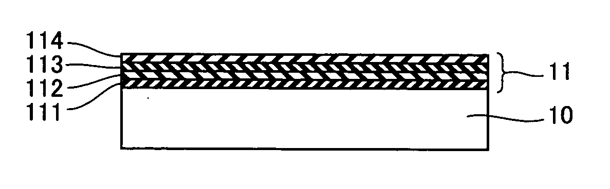
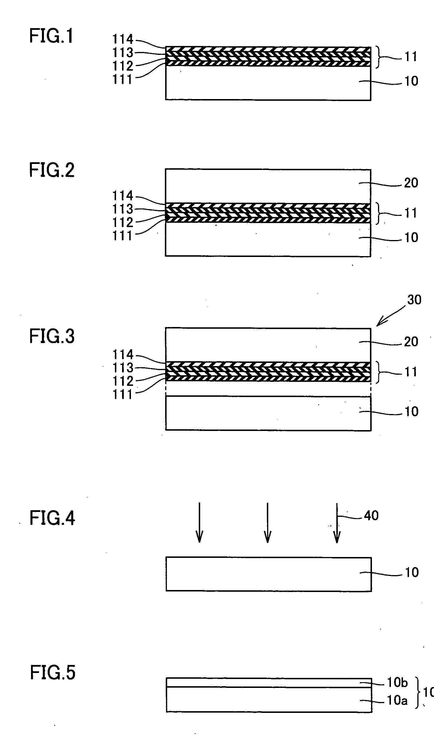
[0036] With reference to FIG. 1, the first substrate 10 implemented by a group III nitride, GaN substrate having a thickness of 1.5 mm is used and MOCVD is employed to deposit semiconductor layer 11 on the GaN substrate heated to 1000° C. Semiconductorlayer 11 is implemented by group III nitride semiconductor layer formed of a p-GaN layer 111 having a thickness of 150 nm, a p-Al0.2Ga0.8N layer 112 having a thickness of 60 nm, an In0.2Ga0.8N layer 113 having a thickness of 3 nm, and an n-GaN layer 114 having a thickness of 5000 nm deposited successively.

[0037] Then, with reference to FIG. 2, on the semiconductor layer 111 outermost, surface layer or n-GaN layer 114, Ag serving as a wax member is sputtered and thus deposited and then melted and the second substrate 20 implemented by a Si substrate having a thickness of 30 μm is stuck thereon. Then, with reference to FIG. 3, a wire saw is used to separate semiconductor layer 111 and the first substrate 10. More specifically, although ...

second example

[0039] Except that the first and second substrates are AlN and Cu substrates, respectively, the wax material is Ni, and the AlN substrate is homoepitaxially grown with AlN used as material, the first substrate has a semiconductor layer deposited thereon, the semiconductor layer has the second substrate stuck thereon, the semiconductor layer and the first substrate are separated, the first substrate separated is surface processed and then homoepitaxially grown, similarly as has been described in the first embodiment. The result is also shown in Table 1.

third embodiment

[0040] Except that the first and second substrates are InN and Cu—W substrates, respectively, the wax material is Ti, The semiconductor layer and the first substrate are separated with an inner, radial blade and the InN substrate is homoepitaxially grown with InN used as material, the first substrate has a semiconductor layer deposited thereon, the semiconductor layer has the second substrate stuck thereon, the semiconductor layer and the first substrate are separated, the first substrate separated is surface processed and then homoepitaxially grown, similarly as has been described in the first embodiment. The result is also shown in Table 1.


PUM

PropertyMeasurementUnit
thicknessaaaaaaaaaa
thicknessaaaaaaaaaa
thicknessaaaaaaaaaa

Abstract

A method of recovering a first substrate, including the steps of: sticking a second substrate on a semiconductor layer epitaxially grown on the first substrate; and separating the semiconductor layer and the first substrate. Furthermore, a method of reproducing a first substrate, including the step of surface processing the first substrate separated. Furthermore, a method of reproducing a first substrate, including the step of homoepitaxially growing the first substrate surface processed. Furthermore, a method of producing a semiconductor wafer, including the step of epitaxially growing a semiconductor layer on a first substrate. Thus a group III nitride or similar, expensive substrate can be used to efficiently and economically, epitaxially grow a group III nitride or similar semiconductor layer.

Description

BACKGROUND OF THE INVENTION [0001] 1. Field of the Invention [0002] The present invention relates generally to methods of efficiently recovering and reproducing substrates and methods of efficiently producing semiconductor wafers. More specifically, the present invention relates to methods of recovering and reproducing a first substrate having a semiconductor layer formed thereon and methods of producing semiconductor wafers including the steps of sticking a second substrate on the semiconductor layer and separating the first substratefrom the semiconductor layer. [0003] 2. Description of the Background Art [0004] To grow a group III nitride semiconductor such as AlxGayIn1-x-yN, wherein 0≦x, 0≦y, and x+y≦1, a sapphire substrate is currently, generally used (see Group III Nitride Semiconductor, edited by Isamu Akasaki, Kabushiki Kaisha Baifukan, Dec. 8, 1999, pp. 93-102, or Naoki Shibata, “Fabrication of LED Based on III-V Nitride and its Applications”, Journal of the Japanese Associ...

Claims


Application Information

Patent Timeline
Patent Type & Authority Applications(United States)
IPC IPC(8): H01L21/02H01L21/20H01L21/30H01L21/46
CPCH01L21/02389H01L21/02425H01L21/02631H01L21/0254H01L21/0262H01L21/02458H01L21/20
Inventor NAKAHATA, SEIJI
Owner SUMITOMO ELECTRIC IND LTD
Why Eureka
Try Eureka