Display device and method for production thereof

a technology of a display device and a production method, applied in the field of display devices, can solve the problems of increasing production costs, deteriorating display quality, and easy oxidation of aluminum in the atmosphere, and achieve the effect of easy production

Active Publication Date: 2008-04-29
KOBE STEEL LTD
View PDF11 Cites 75 Cited by
  • Summary
  • Abstract
  • Description
  • Claims
  • Application Information

AI Technical Summary

Benefits of technology

[0008]The conventional technology mentioned above necessitates the presence of barrier metal in order to avoid direct contact between signal lines (formed from aluminum or aluminum alloy) and the transparent conductive film because direct contact increases contact resistance and deteriorates display quality. This problem arises from the fact that aluminum is easily oxidized by oxygen in the atmosphere and also by oxygen which is released or added when the transparent conducive film (in the form of metal oxide) is formed. This oxidation forms a surface layer of high-resistance aluminum oxide. The insulation layer thus formed in the interface between the signal lines and the transparent conductive film increases the contact resistance between them and deteriorates the display quality.
[0009]Barrier metal is originally intended to protect aluminum alloy from surface oxidation and to achieve good contact between the aluminum alloy film and the transparent conductive film. The conventional structure (having barrier metal formed on the contact interface) inevitably needs a barrier metal forming step. This means that the production facility needs a chamber to form the barrier metal film in addition to the sputtering apparatus to form the gate, source, and drain electrodes. Such an additional apparatus increases production cost and decreases productivity to an unignorable extent in mass production of low-price liquid crystal panels.
[0012]The present inventors continued their investigation for further improvement from a different point of view. It is an object of the present invention to provide a technology for aluminum alloy wiring which will realize a contact superior in stability and long-term reliability to that of the previously filed technology.
[0019]The display device according to the present invention can be produced easily by forming an aluminum alloy film on a substrate and then forming a transparent conductive film on the aluminum alloy film in two steps. The first step is carried out in a non-oxidizing atmosphere, with the substrate kept at a high temperature. The second step is carried out in an oxygen-containing atmosphere.
[0020]The present invention realizes direct contact (without barrier metal) between the aluminum alloy film and the transparent conductive film under stable control. Thus it economically provides a display device excelling in performance and long-term reliability.

Problems solved by technology

This problem arises from the fact that aluminum is easily oxidized by oxygen in the atmosphere and also by oxygen which is released or added when the transparent conducive film (in the form of metal oxide) is formed.
The insulation layer thus formed in the interface between the signal lines and the transparent conductive film increases the contact resistance between them and deteriorates the display quality.
Such an additional apparatus increases production cost and decreases productivity to an unignorable extent in mass production of low-price liquid crystal panels.
This demand, however, is not met by the technologies disclosed in Patent Documents 2 and 3 mentioned above.
The technology disclosed in Patent Document 1 requires the replacement of ITO film (which is most common at the present time) by IZO film, and this leads to an increase in material cost.

Method used


Image

  • Display device and method for production thereof
  • Display device and method for production thereof
  • Display device and method for production thereof

Examples


examples

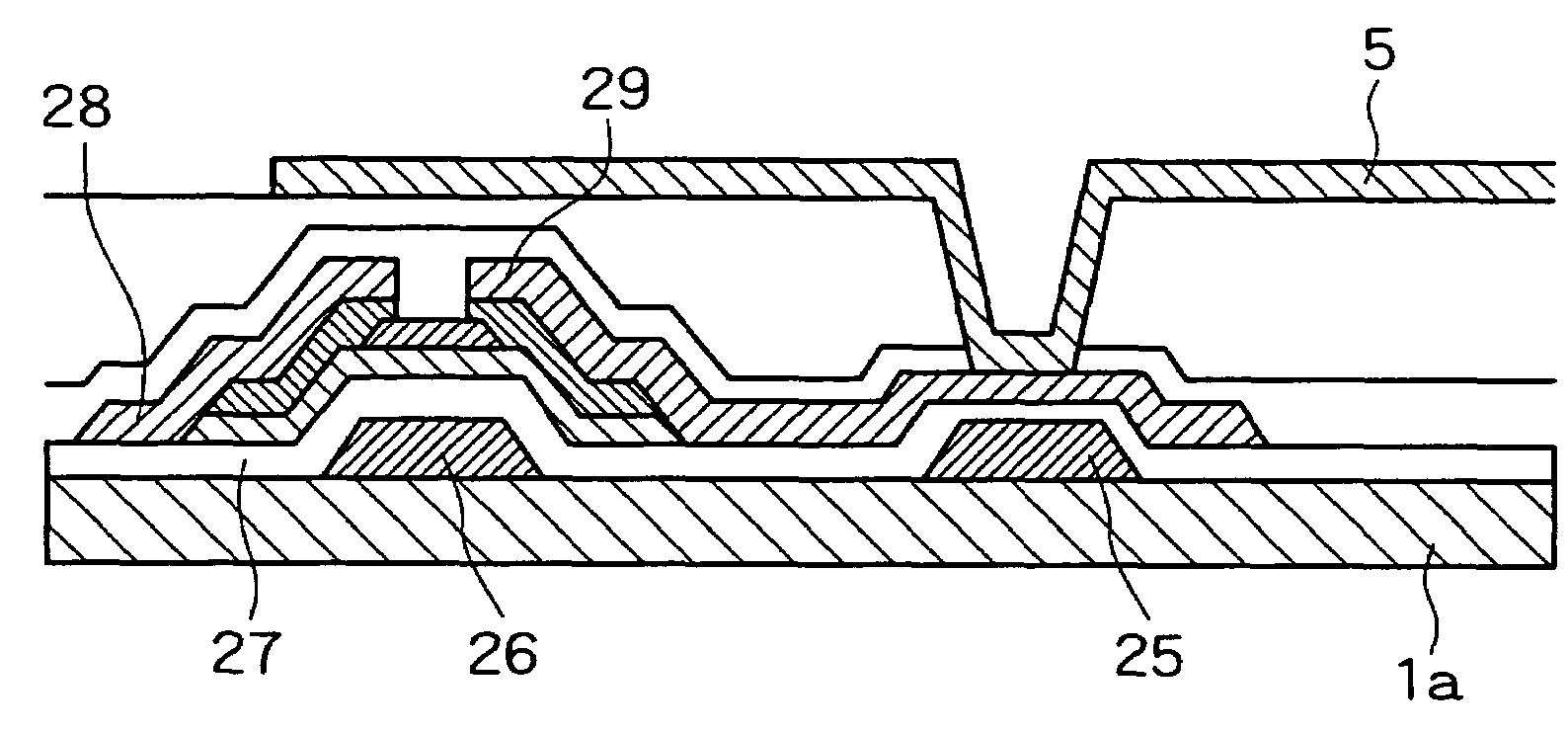
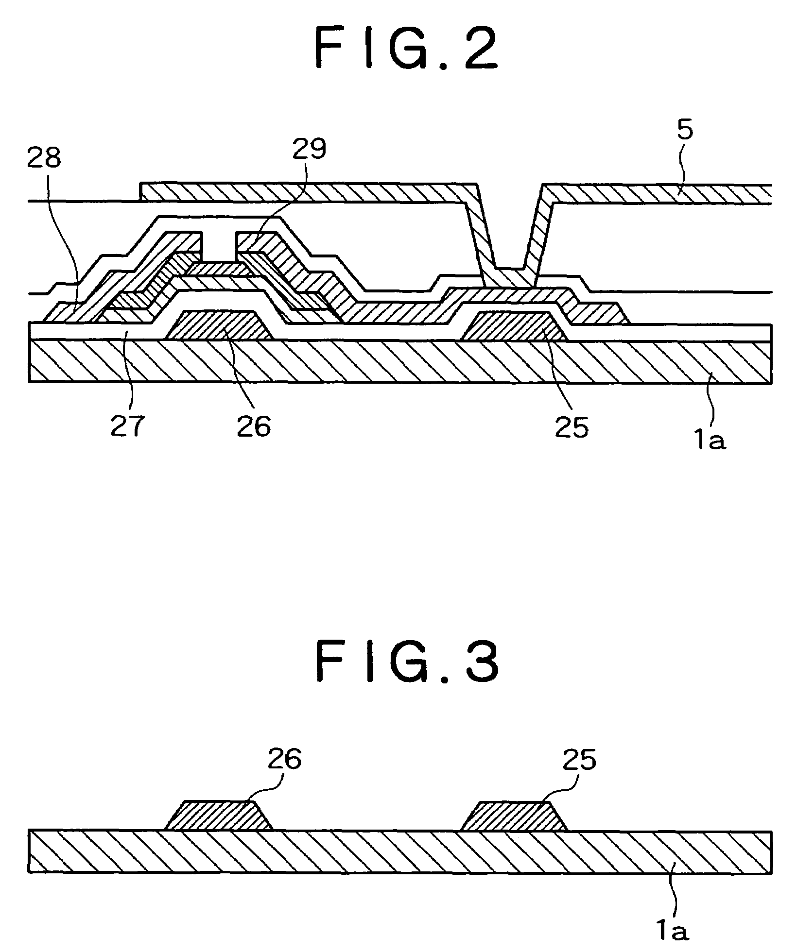
[0128]Table 1 shows the results of measurements of contact resistance between the transparent conductive film 5 (on the substrate with TFT array) and the aluminum alloy film, which are in direct contact with each other.

[0129]The experiments for measurements were carried in the following manner.[0130](1) Constitution of transparent conductive film: Indium tin oxide (ITO) composed of indium oxide and 10 wt % of tin oxide; or indium zinc oxide (IZO) composed of indium oxide and 10 wt % of zinc oxide. The film thickness is 200 nm in both cases.[0131](2) Constitution of aluminum alloy film: Aluminum alloy containing 2 atom % of Ni; or aluminum alloy containing 2 atom % of Ni and 0.6 atom % of Nd.[0132](3) Formation of transparent conductive film:

Condition A in the Initial Stage of Formation.

[0133]Atmosphere gas: argon

[0134]Pressure: 3 mTorr

[0135]Sputter power density: 1.9 W / cm2

[0136]Film thickness: 20 nm

Condition B in the Later Stage of Formation:

[0137]Atmosphere gas: argon / oxygen mixed...


PUM

PropertyMeasurementUnit
thicknessaaaaaaaaaa
thicknessaaaaaaaaaa
thickaaaaaaaaaa

Abstract

A display device and a method for production thereof. The display device comprises a substrate, thin film transistors and a transparent conductive film which are formed on the substrate, and an aluminum alloy film which electrically connects the thin film transistors to the transparent conductive film, such that there exists an oxide film of said aluminum alloy at the interface between said aluminum alloy film and said transparent conductive film, said oxide film having a thickness of 1 to 10 nm and containing oxygen in an amount no more than 44 atom %. The display device has the aluminum alloy film and the transparent conducive film in direct contact with each other, obviating the necessity of barrier metal between them.

Description

BACKGROUND OF THE INVENTION[0001]1. Field of the Invention[0002]The present invention relates to a display device in thin film form and a method for production thereof. More particularly, the present invention relates to a new display device including a transparent conductive film and an aluminum alloy film as constituents, which are used for flat panel displays (such as liquid crystal display) of active or passive matrix type, reflecting film, and optical parts, and a method for production thereof.[0003]2. Description of the Related Art[0004]A liquid crystal display device of active matrix type is composed of two mutually opposing substrates and a liquid crystal layer held between them. It relies on thin film transistors (TFT) as switching devices. The first substrate has a transparent conductive film and an array of TFTs connected to scanning lines and signal lines. The second substrate, which is a certain distance away from the first one, has a common electrode. By contrast, a li...

Claims


Application Information

Patent Timeline
Patent Type & Authority Patents(United States)
IPC IPC(8): G02F1/133
CPCG02F1/136227G02F1/1368G02F1/136
Inventor GOTOH, HIROSHIKUGIMIYA, TOSHIHIROTOMIHISA, KATSUFUMINAKAI, JUNICHI
Owner KOBE STEEL LTD
Why Eureka
Try Eureka