CMOS light sensing cell

a light sensing cell and cmos technology, applied in the field of integrated cmos light sensing arrays, can solve the problems of slow charge of capacitor c, capacitor cb>1/b>, and no longer negligible parasitic voltag

Active Publication Date: 2005-02-24
STMICROELECTRONICS SRL
View PDF3 Cites 39 Cited by
  • Summary
  • Abstract
  • Description
  • Claims
  • Application Information

AI Technical Summary

Problems solved by technology

A drawback of the above light sensing cell is due to the thermal noise in the transistor T3, which causes capacitor C1 to be charged with a random low parasitic voltage at the opening of transistor T3.
However, if the sensor receives only a small quantity of light and supplies a low sensing current Is, the capacitor C1 charges slowly and the parasitic voltage is no longer negligible compared to t...

Method used


Image

  • CMOS light sensing cell
  • CMOS light sensing cell
  • CMOS light sensing cell

Examples


Embodiment Construction

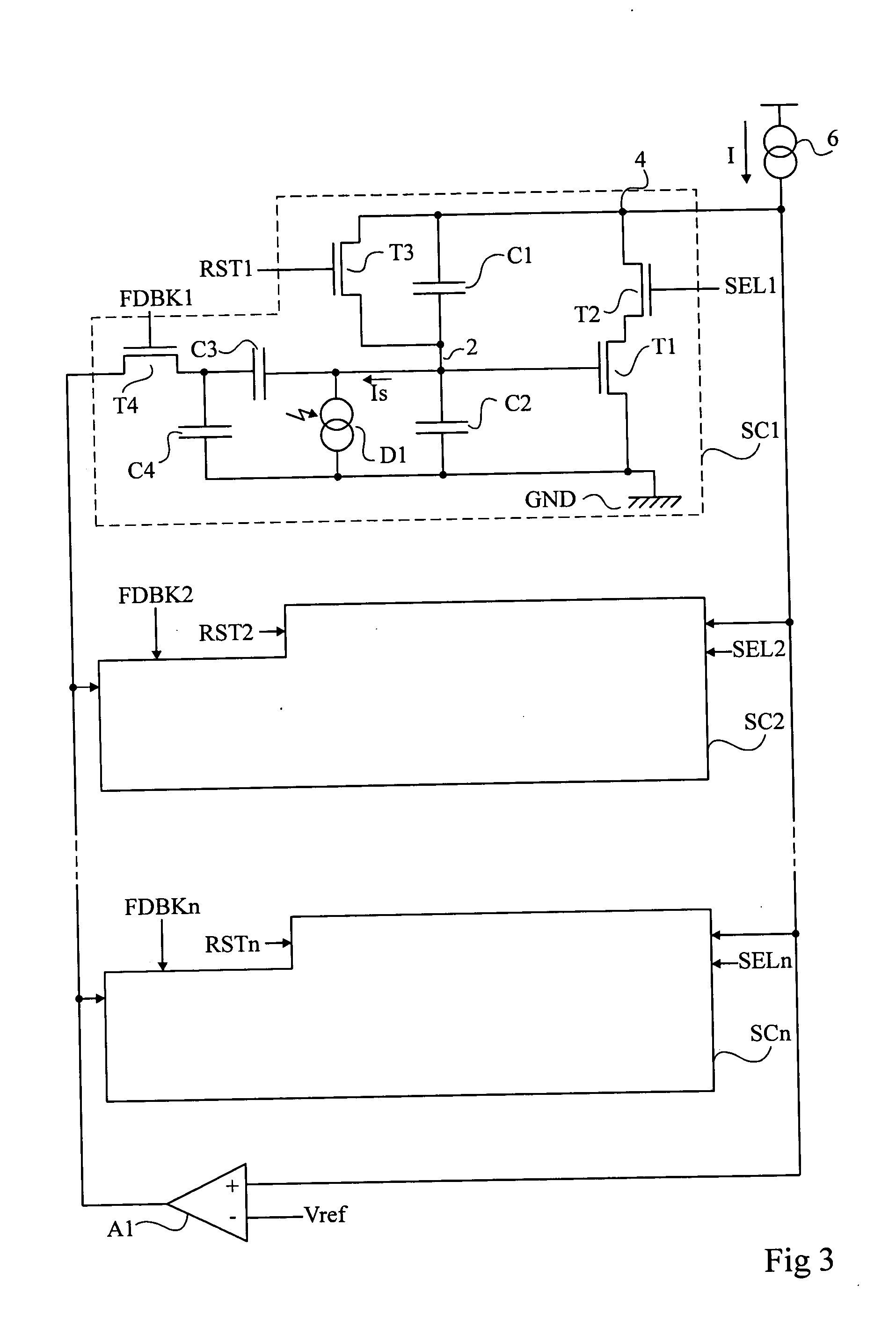
[0030] Same reference numbers correspond to same elements in the different figures. For clarity's sake, only the elements that are useful to the understanding of the invention have been illustrated.

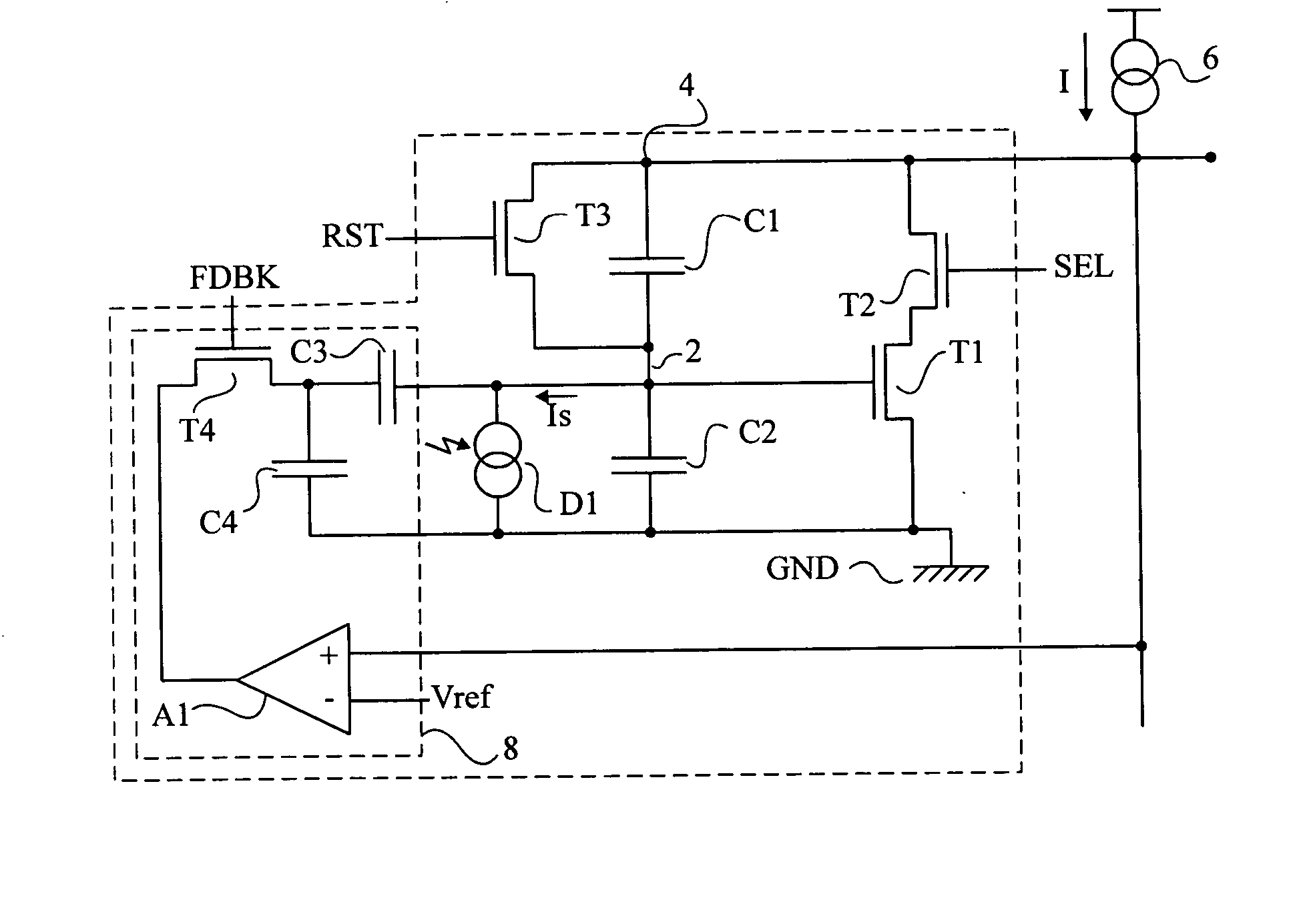
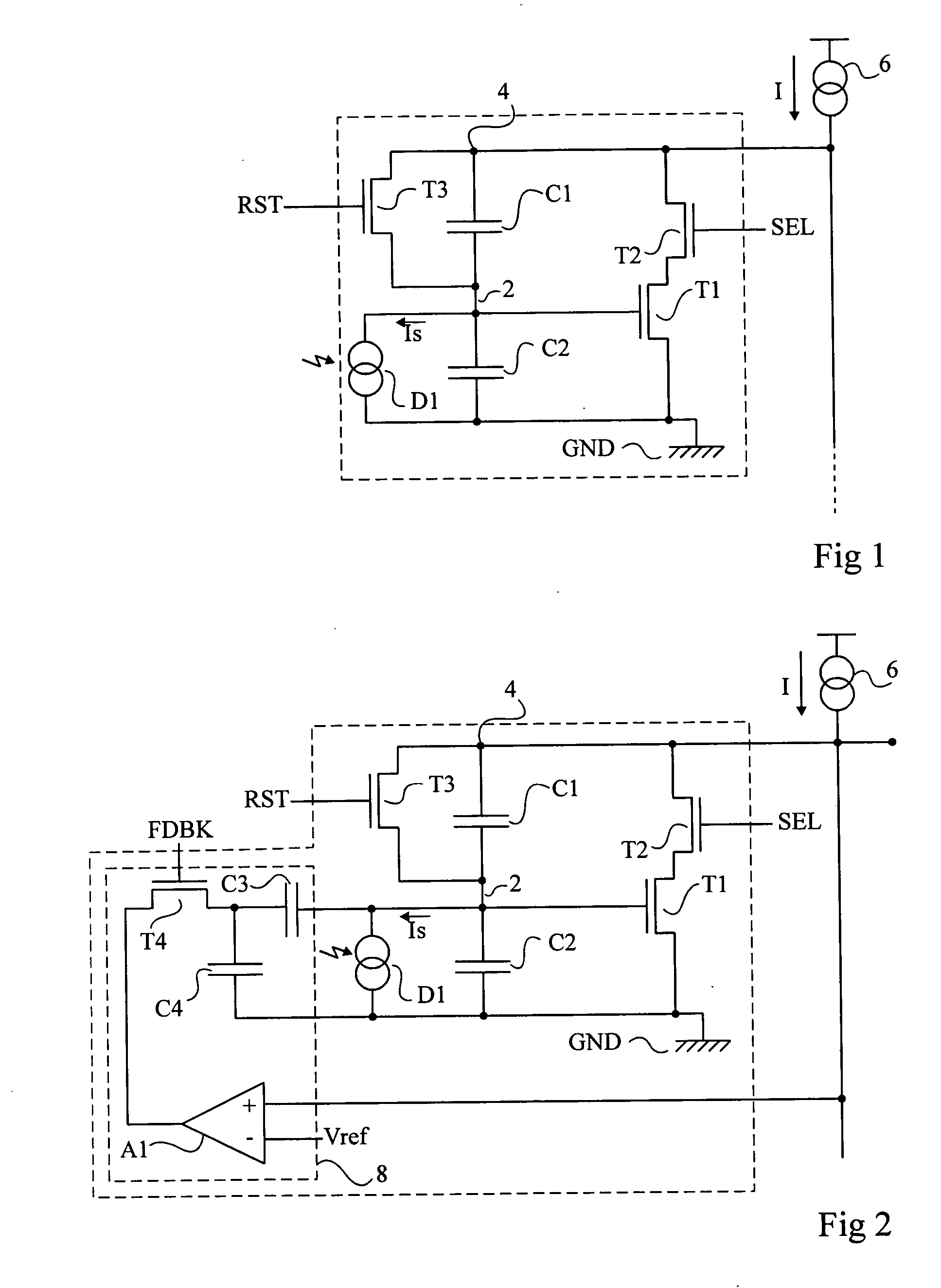
[0031]FIG. 2 schematically represents a CMOS light sensing cell illustrating an aspect of the invention, comprising a sensor D1, capacitors C1 and C2, and CMOS transistors T1, T2 and T3, connected as in FIG. 1.

[0032] The sensing cell further comprises a feedback block 8 comprised of an operational amplifier A1, capacitors C3 and C4 and a MOS transistor T4 of N-channel type. The non-inverting and inverting input of the operational amplifier A1 are respectively connected to the output node 4 and to a reference voltage Vref that will be described later. The output of the operational amplifier A1 is connected to the source of transistor T4. The gate of transistor T4 is connected to a non-illustrated control block supplying a feedback control signal FDBK. The drain of transistor T4 is connec...


PUM


Abstract

A light sensing cell comprising output means (T1, T2) for generating an output voltage depending on the voltage of a sensing node (2), the voltage of the sensing node varying as a function of a received light; a reset transistor (T3) operable to force the voltage of the sensing node (2) to a reset voltage; a feedback loop comprising an operational amplifier (A1) operable to add through a capacitive voltage divider (C3, C4) a correction voltage to the voltage of the sensing node (2), said correction voltage depending on the output voltage; and preset means (T5) for, during the operation of the reset transistor (T3) and until the amplifier (A1) is operated, setting the input of the capacitive voltage divider (C3, C4) to a predetermined voltage (Vinit).

Description

BACKGROUND OF THE INVENTION [0001] 1. Field of the Invention [0002] The invention relates to integrated CMOS light sensing arrays comprising light sensing cells, and in particular to the structure of the light sensing cells. [0003] 2. Discussion of the Related Art [0004] CMOS light sensing arrays integrated on chips are widely used in modem imaging devices such as digital cameras or scanners. A light sensing array typically comprises light sensing cells, or pixels, arranged in rows and columns. [0005]FIG. 1 represents a typical light sensing cell of a non-illustrated CMOS light sensing array composed of cells arranged in rows and columns. Such a light sensing cell is for example described in C. Staller et al., “A radiation hard, low background multiplexer design for spacecraft imager applications” in Infrared Readout Electronics, Proc. SPIE, Vol. 1684, pp. 175-181 (1992). The cell comprises a sensor D1, capacitors C1 and C2, and CMOS transistors T1, T2 and T3 of N-channel type. The ...

Claims


Application Information

Patent Timeline
IPC IPC(8): H01L27/146H04N5/363H04N5/3745
CPCH01L27/14609H04N5/3745H04N5/363H04N25/65H04N25/77
Inventor LULE, TAREKBENTHIEN, STEPHAN
Owner STMICROELECTRONICS SRL
Why Eureka
Try Eureka