Optical semiconductor device

a technology of optical semiconductors and semiconductors, applied in the direction of semiconductor devices, basic electric elements, electrical equipment, etc., can solve the problems of inability to use light and attenuation of light, and achieve the effect of suppressing power consumption and enhancing brightness

Active Publication Date: 2005-02-24
ROHM CO LTD
View PDF4 Cites 7 Cited by
  • Summary
  • Abstract
  • Description
  • Claims
  • Application Information

AI Technical Summary

Benefits of technology

[0010] The present invention has been conceived under the circumstances described above. It is therefore an object of the present invention to provide a compact optical semiconductor device which is capable of enhancing the brightness while suppressing an increase in the power consumption.

Problems solved by technology

However, the semiconductor device B still has a room for improvement for enhancing the brightness, because the semiconductor device B has the following problems.
Such light is attenuated while undergoing repetitive reflection within the optical semiconductor device B and cannot be utilized as light for illumination.

Method used


Image

  • Optical semiconductor device
  • Optical semiconductor device
  • Optical semiconductor device

Examples


Embodiment Construction

[0027] Preferred embodiments of the present invention will be described below with reference to the accompanying drawings.

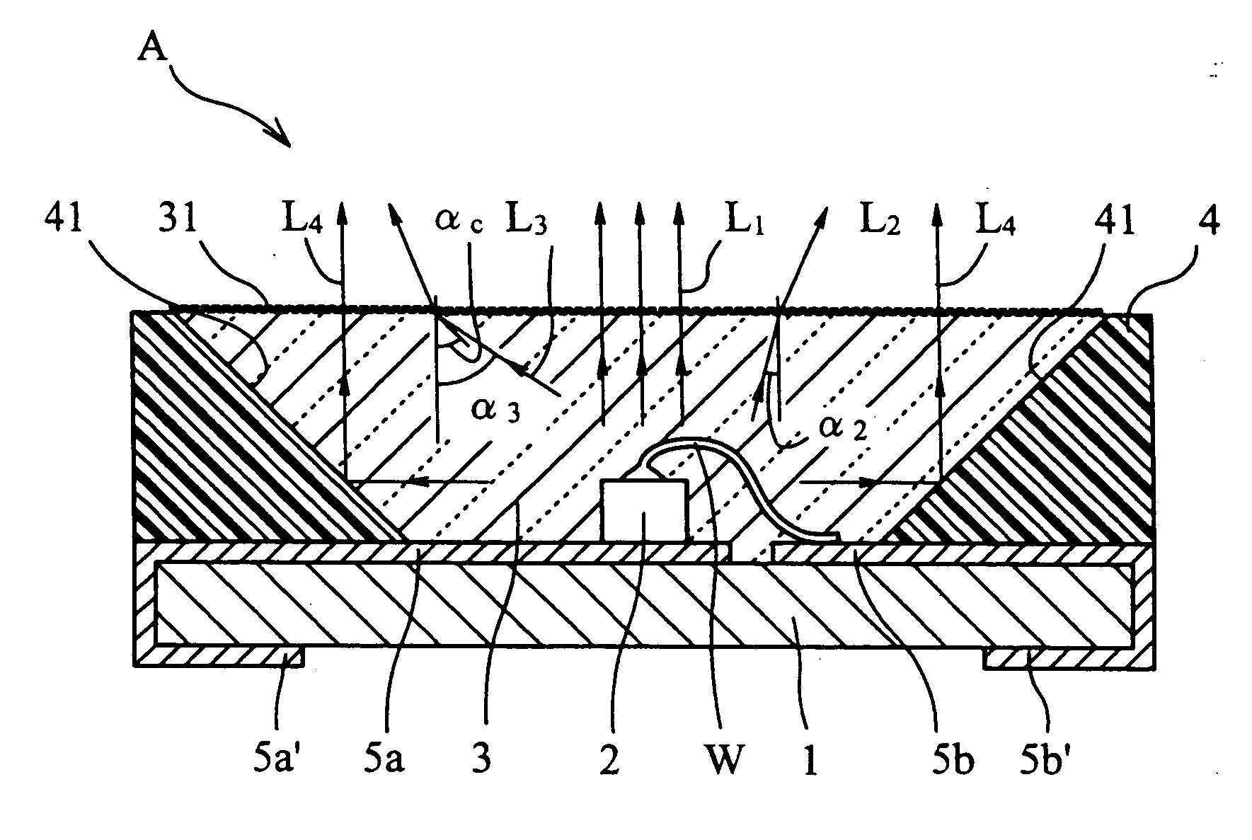
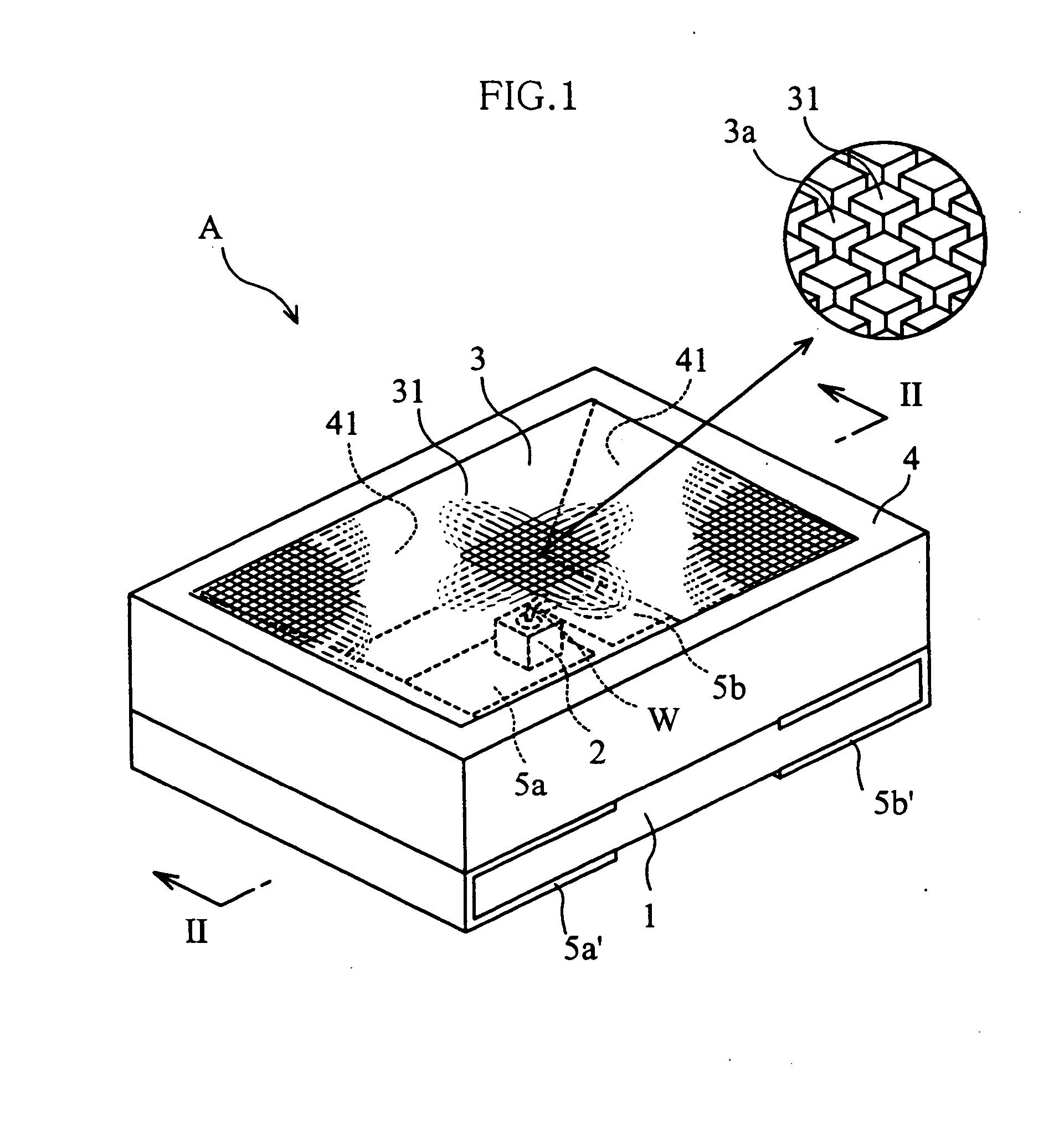
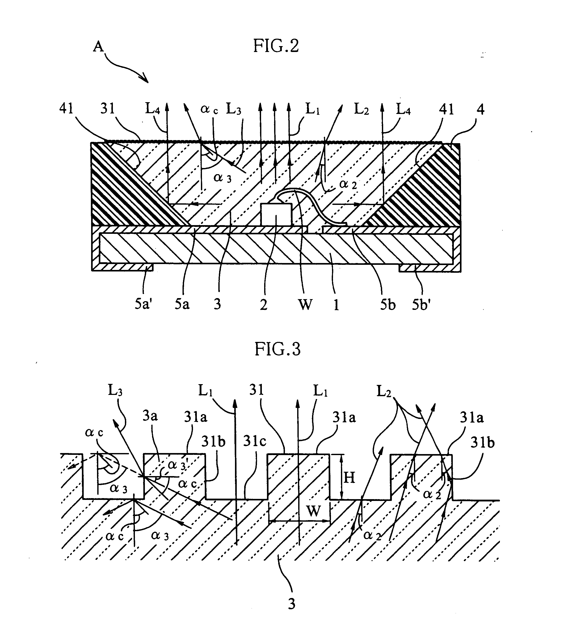
[0028]FIG. 1-3 illustrate an optical semiconductor device according to the present invention. The illustrated optical semiconductor device A includes a substrate 1, an LED chip 2, a light permeable member 3 and a reflector 4.

[0029] The substrate 1 comprises a flat insulating plate having an upper surface and a lower surface which are rectangular and extend in parallel with each other. The substrate 1 is made of a glass-fiber-reinforced epoxy resin, for example. The LED chip 2, the light permeable member 3 and the reflector 4 are mounted on the upper surface of the substrate 1. As shown in FIG. 2, on the substrate 1 are formed a first conductor 5a and a second conductor 5b each of which extends from the upper surface up to the lower surface of the substrate 1. The first conductor 5a includes a surface-mounting terminal 5a′ located on the lower surface of the sub...


PUM


Abstract

An optical semiconductor device includes an optical semiconductor chip and a light permeable member covering the optical semiconductor chip. The light permeable member has a light emitting surface for emitting light coming out from the optical semiconductor chip to the outside. The light emitting surface includes a plurality of standing surfaces standing in a second direction which intersects a first direction in which the light emitting surface spreads.

Description

BACKGROUND OF THE INVENTION [0001] 1. Field of the invention [0002] The present invention generally relates to an optical semiconductor device provided by utilizing an optical semiconductor chip such as an LED chip. [0003] 2. Description of the Related Art [0004] A light emitting diode (LED) has advantages such as small power consumption, small size and long lifetime. Therefore, an optical semiconductor device incorporating an LED chip can be advantageously used as a light source for the display of a cellular phone or a notebook computer, for example. Such an optical semiconductor device is so designed as to enhance the brightness. For example, JP-A-2000-183407 discloses the provision of an optical reflector surrounding the LED chip. [0005]FIG. 8 shows an optical semiconductor device as a related art of the present invention. The illustrated semiconductor device B includes a substrate 101, an LED chip 102 mounted on the substrate, and a light permeable member 103 covering the LED ch...

Claims


Application Information

Patent Timeline
Patent Type & Authority Applications(United States)
IPC IPC(8): H01L27/15H01L33/22H01L33/54H01L33/56H01L33/60H01L33/62
CPCH01L33/54H01L2933/0091H01L2224/48091H01L2224/48465H01L2924/00014H01L2924/00
Inventor ISOKAWA, SHINJI
Owner ROHM CO LTD
Why Eureka
Try Eureka