
Optical packet buffering device and buffering method thereof

a buffering device and optical packet technology, applied in data switching networks, multiplex communication, digital transmission, etc., can solve the problems of limited buffering speed, increased size of optical elements, and inability to use practicable optical logic circuits, so as to increase data processing speed and simplify calculation and implementation in hardware.

Inactive Publication Date: 2005-02-24
NAT INST OF INFORMATION & COMM TECH
View PDF1 Cites 29 Cited by
  • Summary
  • Abstract
  • Description
  • Claims
  • Application Information

AI Technical Summary

Benefits of technology

As described above, when the period T is 2p (where p is an integer) times or 2nk times the delay time D, this invention simplifies the implementation in hardware by eliminating division, and can further increase the speed of data processing.
As described above, since arrival gap time is always zero and packet length is unity in the case of synchronously-arriving fixed-length packets, this invention simplifies the calculation and the implementation in hardware, and can further increase the speed of data processing.

Problems solved by technology

This is because practical optical logic circuits had not been available.
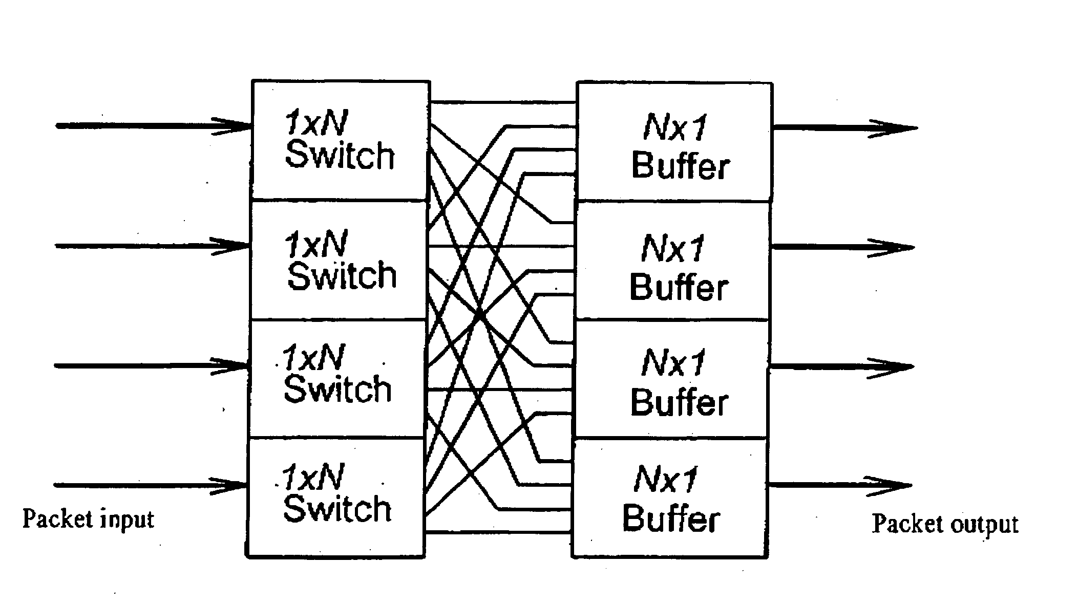
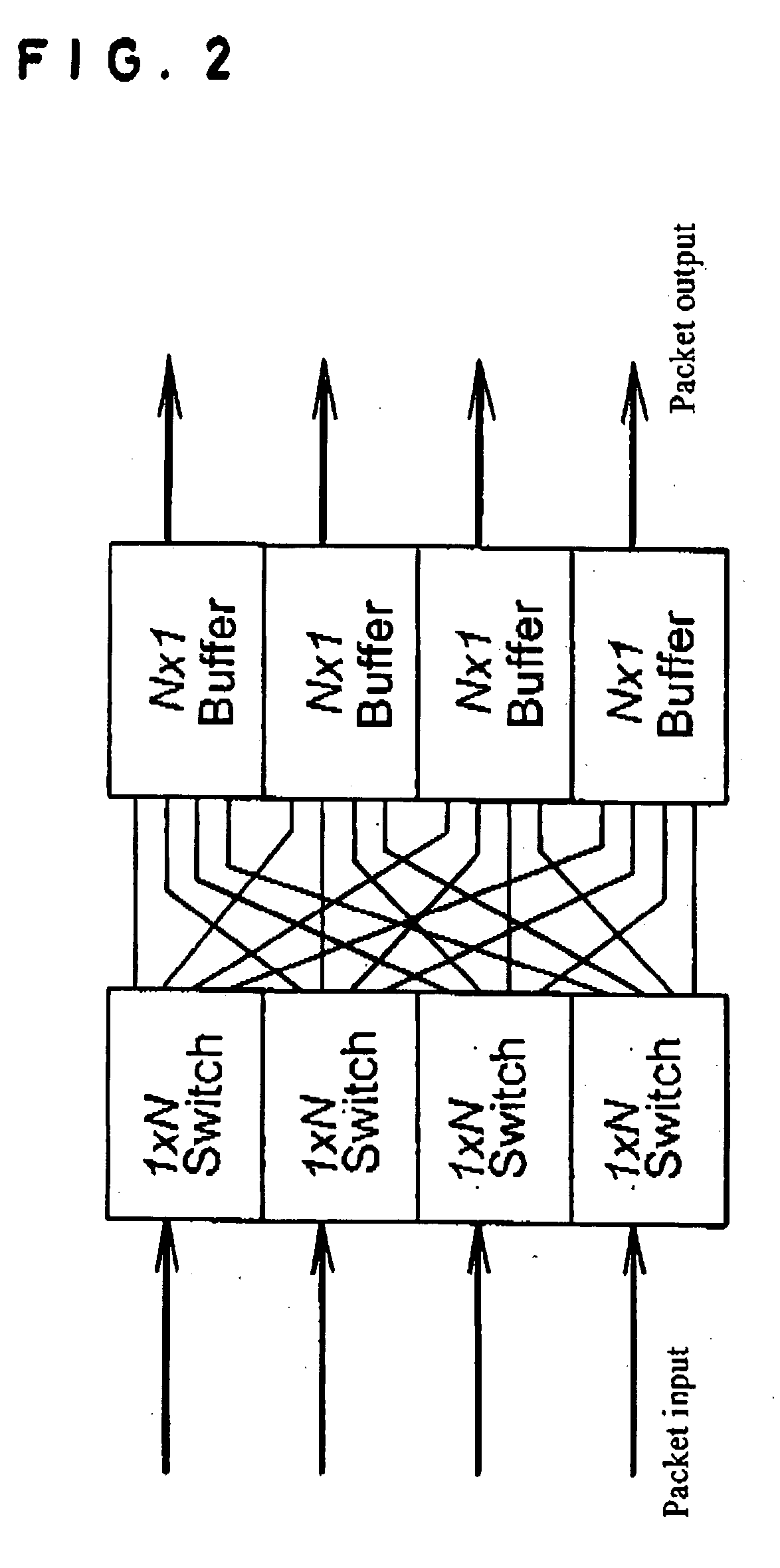
Taking N to be the number of ports, this increases the processing speed by N1 / 2 times in comparison to the round robin processing described above, but a group of delay lines must be placed at each buffer unit so the increased size of the optical element is a problem.
The round-robin scheme described above proceeds sequentially, with data processing regarding buffering being performed in a predetermined port order, so in order to perform high-speed buffering, it is necessary to perform the data processing at high speed but thus the buffering speed is limited.

Method used


Image

  • Optical packet buffering device and buffering method thereof
  • Optical packet buffering device and buffering method thereof
  • Optical packet buffering device and buffering method thereof

Examples


example 1

The main point of the present invention is to determine the delay times for as many packets as possible per time unit. To this end, a large number of processors Pij are disposed as shown in FIG. 13 to perform the processing required to determine the delay times in parallel. Here, Pij refers to the processor provided on the ith stage of the jth lightpath. In order to be particularly clear, Pij may be represented as P(i,j).

In FIG. 13, the length l (L) of the optical packet signals of the eight lightpaths from IN1 to IN8 and the interval (packet pre-period) t from the optical packet signal to the clock signal are used to perform coordination so that the percentage of optical packets discarded is minimized. In this case also, delay elements that are arranged with equal differences between their delay times are shown, and the Δn serving as the output is shown as a coefficient of the base delay time of D. In FIG. 13, the circles indicate processors and the squares are registers R. Here...

example 2

In order to perform the processing of the flowcharts above at high speed, it is preferably implemented in semiconductor circuits (hardware). However, in order to implement it in hardware, the processing procedure must be described in hardware description language (HDL) and converted to circuitry, but the function (max) that finds the maximum value is used in Table 6 above, yet this operate cannot be used in the current state. In addition, division is used in the above processing procedure and this may complicate the circuitry, or cause the processing to slow down, among other problems. These problems are solved by setting T=2pD (where p is an integer).

In this case, the first-stage processors P1n perform processing according to the flowchart shown in FIG. 21. If this processing were written in the form of a program, it would be as follows.

TABLE 8First Stage (P1n: 1≦n≦8)ln , ln−1: packet lengthtn , tn−1: arrival gap timegn−1: temporary variable for queue lengthfn,1 , tn,1 : outpu...

example 3

When the above buffering device in the optical packet switch for asynchronous variable-length optical packets is used for buffering in an optical packet switch for synchronous fixed-length optical packets, the parallel processing of FIG. 26 can be simplified to give the constitution of FIG. 27. Similarly, in the same manner as the constitution illustrated in FIG. 13, with the constitution using the dotted-line portion that sequentially sends data forward, the variables can be set to those of synchronous fixed-length to give the constitution of FIG. 28. In FIGS. 27 and 28, the number of variables used in processing is reduced. The number of variables can be reduced because all of the optical packet lengths become identical, so it is possible to use the number of optical packets instead of the optical packet length in the above process. In addition, the respective optical packets are synchronized, so the processing of the pre-period of optical packets can be omitted. The processing t...


PUM


Abstract

A device that accepts input of asynchronously-arriving variable-length optical packets transmitted over a plurality of lightpaths, and outputs same to a single optical path, comprising: in order to prevent the optical packets from overlapping in the output lightpath, a controller that uses the delay times of the delay elements and the optical packet length and arrival gap time thus read to determine by computation the delay element used for temporary storage, where a plurality of stages of processors is provided. Thus, the processing required to determine the delay time is performed by parallel processing with the results of processing the prefix-sum operation used in parallel pipelined processing along with the queue length, optical packet length and arrival gap time of the buffering device.

Description

BACKGROUND OF THE INVENTION 1. Field of the Invention The present invention relates to an optical packet buffering device that uses optical circuits that have limited buffer capacity or data holding time, in order to guide a plurality of optical packets such that they are not overlapped toward one lightpath, and to the buffering method thereof. 2. Description of the Prior Art With advances in optical communications technology able to transfer large amounts of information, in order to achieve even higher levels of throughput, optical technology is being introduced into not only the transmission paths but also into optical packet switching. Typically in optical packet switching, an optical packet transfer process is performed and an optical packet switch is used therein. The functions of such an optical packet switch can be divided into the five categories of: (1) label lookup, (2) switching, (3) buffer management, (4) buffering and (5) routing. Typically, an optical packet switch...

Claims


Application Information

Patent Timeline
Patent Type & Authority Applications(United States)
IPC IPC(8): H04B10/07H04B10/27H04B10/291H04J14/00H04L12/70H04Q11/00
CPCH04Q2011/002H04Q11/0005
Inventor HARAI, HIROAKI
Owner NAT INST OF INFORMATION & COMM TECH
Learn More