Circuit board and method of manufacturing the same

a technology of circuit board and circuit pattern, which is applied in the field of circuit board, can solve the problems of not teaching at all about incorporating electronic components in the circuit board per se, and the tendency to occur so as to prevent short circuits between circuit pattern routings

Inactive Publication Date: 2005-03-03
PANASONIC CORP
View PDF10 Cites 30 Cited by
  • Summary
  • Abstract
  • Description
  • Claims
  • Application Information

AI Technical Summary

Benefits of technology

The foregoing structure allows forming the circuit patterns in the grooves formed on the surface of the insulating resin layer, so that routings of the pattern are positively isolated by the insulating resin layer. As a result, short circuits between the routings of the circuit pattern can be prevented. The electrodes of the electronic component press-fitted from the back face of the insulating resin layer become positively conductive with the circuit pattern at the bottom of the grooves. This preparation allows a narrower pitch between the routings of the circuit pattern of the circuit board incorporating the electronic components.

Problems solved by technology

However, this utility model does not teach at all about incorporating electronic components in the board per se.
However, since circuit patterns with narrow pitches are formed on the flat face of the circuit board manufactured by this method, a short circuit tends to occur between the circuit patterns.

Method used


Image

  • Circuit board and method of manufacturing the same
  • Circuit board and method of manufacturing the same
  • Circuit board and method of manufacturing the same

Examples


exemplary embodiment 1

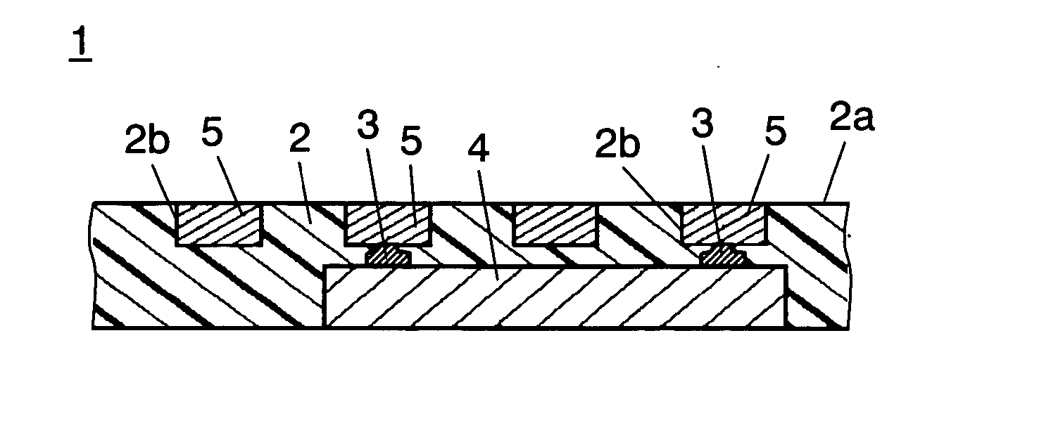
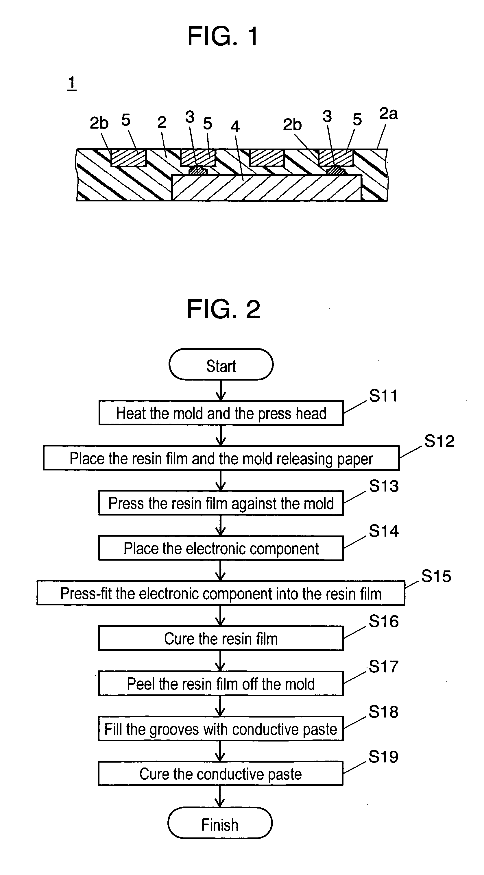
The circuit board and the method of manufacturing the same board in accordance with the first embodiment of the present invention are demonstrated with reference to FIG. 1 through FIG. 10. FIG. 1 shows a sectional view of a circuit board in accordance with the first exemplary embodiment of the present invention. FIG. 2 shows a flowchart illustrating steps of a manufacturing method of the circuit board in accordance with the first embodiment. FIG. 3 through FIG. 10 show sectional views illustrating respective steps of the manufacturing method of the circuit board in accordance with the first embodiment.

Circuit board 1 shown in FIG. 1 comprises the following elements: insulating resin layer 2 of which surface 2a has grooves 2b corresponding to circuit patterns; electronic component 4 disposed inside insulating resin layer 2 and electrode terminals 3 of the component are exposed from a bottom (a section generally understood as a bottom) of grooves 2b; and circuit patterns 5 forme...

exemplary embodiment 2

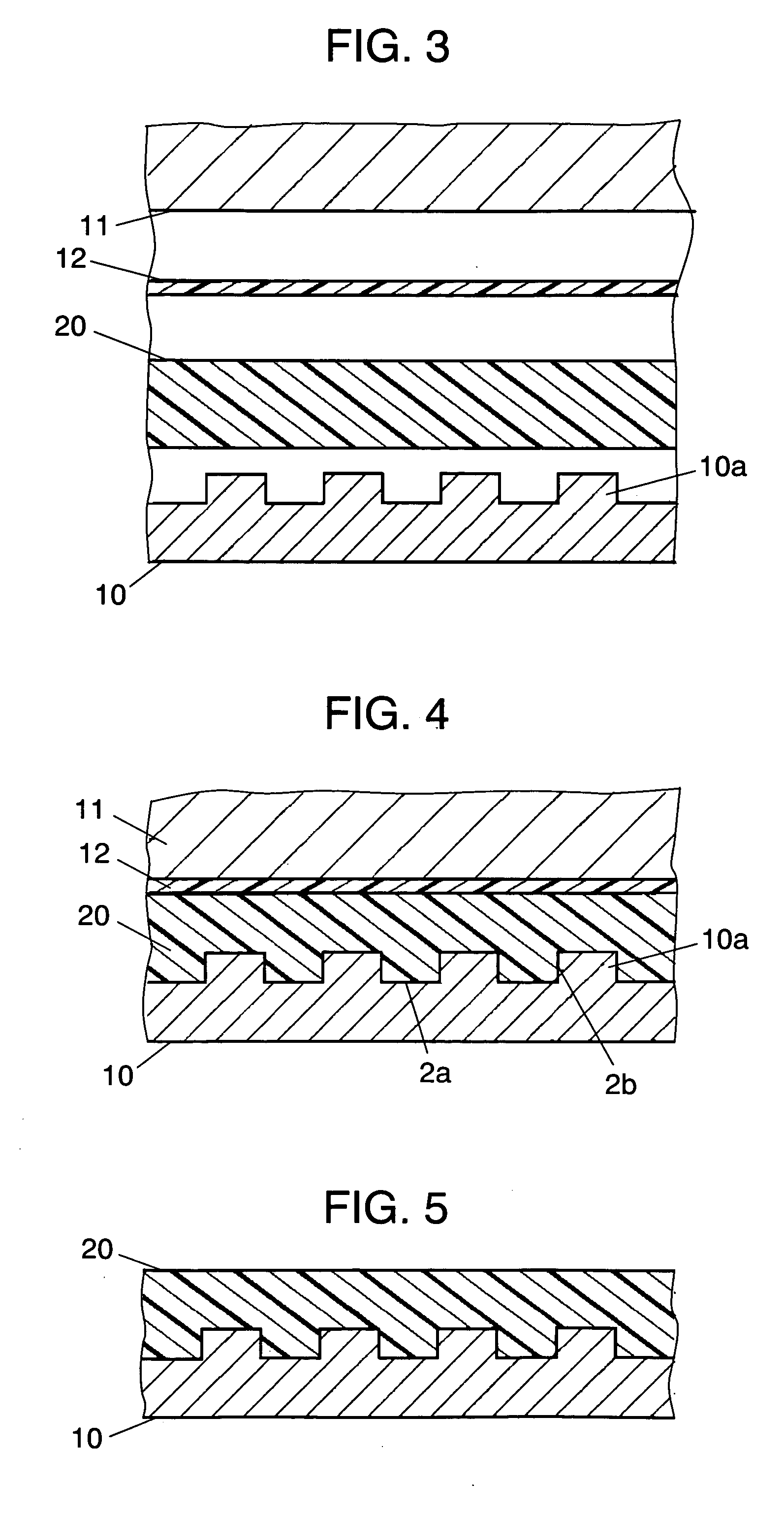
The manufacturing method in accordance with the second exemplary embodiment of the present invention is demonstrated hereinafter with reference to FIG. 11-FIG. 14. Steps common to those of the first embodiment are described with reference to FIG. 2 and FIG. 4 already described in the first exemplary embodiment. This manufacturing method relates to a method of manufacturing a circuit board of which insulating resin layer is formed of thermoplastic resin. FIG. 11 shows a flowchart illustrating steps of the manufacturing method in accordance with the second embodiment. FIG. 12-FIG. 14 show sectional views illustrating respective steps of the manufacturing method. Similar elements to those in the first embodiment have the same reference marks. Steps S11-S13 described in the first embodiment are common to this second embodiment, thus the flowchart in FIG. 11 only shows the steps after step S13.

As shown in FIG. 4, press thermoplastic resin film 20, which is to be insulating resin layer...

exemplary embodiment 3

The manufacturing method in accordance with the third exemplary embodiment of the present invention is demonstrated hereinafter with reference to FIG. 15-FIG. 19. Steps common to those of the first embodiment are described with reference to FIGS. 1, 2 and 9 already described in the first embodiment. FIG. 15 shows a flowchart illustrating steps of the manufacturing method in accordance with the third embodiment. FIG. 16-FIG. 19 show sectional views illustrating respective steps of the manufacturing method. Similar elements to those in the first and second embodiments have the same reference marks. In the manufacturing method shown in FIG. 15, insulating resin layer 2 of circuit board 1 is not limited to thermoplastic resin, but thermosetting resin or photo-setting resin can be used.

First, as shown in FIG. 16, place resin film 20, which is to be insulating resin layer 2, on base plate 16. At this time, if film 20 is made from thermoplastic resin, heat film 20 via base plate 16 up t...


PUM

PropertyMeasurementUnit
softening pointaaaaaaaaaa
thicknessaaaaaaaaaa
thicknessaaaaaaaaaa

Abstract

Apply heat to thermoplastic resin film, which is eventually to become an insulating resin layer, and press the film against a mold for forming grooves on a surface of the film. Next, press-fit an electronic component into the resin film from a back-face of the film, thereby exposing electrodes of the component from a bottom of the grooves. Then cool the film for curing. Peel the film off the mold, then fill the grooves with conductive paste, and cure the paste for forming circuit patterns. The foregoing procedure allows bringing the electrodes positively into conduction with the circuit patterns of a circuit board incorporating the electronic component, and achieving a narrower pitch between routings of the circuit patterns.

Description

FIELD OF THE INVENTION The present invention relates to a circuit board incorporating electronic components and a method of manufacturing the same circuit board. BACKGROUND OF THE INVENTION In recent years, narrower pitches of circuit patterns of circuit boards have been required in the market in order to increase a board density. In parallel with this tendency, a circuit board incorporating electronic components therein is proposed. The circuit board incorporating electronic components, in particular, is required to have a further narrower pitch in circuit patterns. Japanese Utility Model Publication No. S62-70473 discloses a method of avoiding short circuits in a circuit having a narrow pitch: forming grooves on an insulated board, and then filling the grooves with conductive paste for forming a circuit, thereby avoiding short-circuits. However, this utility model does not teach at all about incorporating electronic components in the board per se. On the other hand, Japanese P...

Claims


Application Information

Patent Timeline
Patent Type & Authority Applications(United States)
IPC IPC(8): H01L21/48H01L21/60H01L23/12H01L23/482H01L23/538H05K1/00H05K1/03H05K1/09H05K1/18H05K3/00H05K3/10H05K3/12
CPCH01L21/4846Y10T29/4913H01L24/18H01L24/82H01L24/97H01L2224/16H01L2224/18H01L2224/76155H01L2224/97H01L2924/01029H01L2924/01033H01L2924/01046H01L2924/01047H01L2924/01075H01L2924/01078H01L2924/01079H01L2924/01082H01L2924/14H01L2924/1815H01L2924/18161H01L2924/19041H01L2924/19043H05K1/095H05K1/185H05K3/107H05K3/1258H05K2201/0129H05K2201/09036H05K2201/10674H05K2203/1189H01L23/5389H01L2224/82102H01L2924/01006H01L2224/82H01L2924/12042H01L2224/04105H01L24/20H01L21/568H01L24/19H01L2924/00
Inventor SAKURAI, DAISUKETSUKAHARA, NORIHITONISHIKAWA, KAZUHIRO
Owner PANASONIC CORP
Why Eureka
Try Eureka