Semiconductor device and method for fabricating the same

a technology of voltage variable capacitor and semiconductor device, which is applied in the direction of semiconductor devices, diodes, electrical apparatus, etc., can solve the problem that the varactor with a short gate length cannot provide the desired varactor performance, and achieve the effect of short gate length and extended depletion layer

Active Publication Date: 2005-03-03
GK BRIDGE 1
View PDF3 Cites 15 Cited by
  • Summary
  • Abstract
  • Description
  • Claims
  • Application Information

AI Technical Summary

Benefits of technology

[0014] In the varactor region Va, the substrate contact impurity diffusion regions 113a and the extension regions 113b serve as substrate contact impurity diffusion regions. Both the substrate contact impurity diffusion regions 113a and the extension regions 113b contain an N-type impurity at a higher concentration than the N well region 112. Therefore, when a voltage (bias) is applied between the polysilicon gate electrode 118 and the substrate contact impurity diffusion regions 113a, a depletion layer formed below the gate is restrained from extending in the direction parallel to the principal surface of the semiconductor substrate 110 (horizontal direction). More particularly, the gate length and width of the polysilicon gate electrode 118 define the extendable range of the depletion layer. Thus, as the gate length of the polysilicon gate electrode of the varactor is shortened in order to downsize the semiconductor device, the extendable range of the depletion layer becomes narrower. Therefore, the capacitance C2 at a reverse bias of zero would increase.
[0018] In this way, there does not exist in the MIS capacitor of the semiconductor device any impurity diffusion region that would conventionally be formed simultaneously with extension regions and LDD regions of the MISFET and contains an impurity at a low concentration. Thus, on application of a gate bias, the extendable range of a depletion layer below a gate electrode can be kept wide enough. Hence, when the MIS capacitor is used as a varactor, the variable capacitance range can be kept wide enough even for reduction in the gate length according to miniaturization in the semiconductor device.
[0021] It is more preferable that the at least one substrate contact region is formed in the second active region only between one side of the gate electrode and one of isolation trenches, because the extendable range of the depletion layer can further be extended.
[0023] It is preferable that each of the MISFET and the MIS capacitor further comprises an offset spacer interposed between its gate electrode and its sidewall, because the extendable range of the depletion layer in the MIS capacitor can further be extended.
[0028] With this method, the MIS capacitor of the semiconductor device is formed with no impurity diffusion region which would conventionally be formed simultaneously with extension regions and LDD regions of the MISFET and contains an impurity at a low concentration. Thus, in the formed semiconductor device, the extendable range of the depletion layer below a gate electrode can be kept wide enough on application of a gate bias. Hence, when the MIS capacitor is used as a varactor, the variable capacitance range can be kept wide enough even for reduction in the gate length according to miniaturization in the semiconductor device.
[0032] According to the semiconductor device and the method for fabricating the same of the present invention, the MIS capacitor is provided with no low-concentration impurity diffusion regions existing in the MISFET. Thus, the depletion layer can be extended and a varactor element having a short gate length can be improved in its performance.

Problems solved by technology

However, the varactor having the above-described known structure formed using the existing CMOS process has the following problem.
A varactor having a short gate length cannot provide desired varactor performance.

Method used


Image

  • Semiconductor device and method for fabricating the same
  • Semiconductor device and method for fabricating the same
  • Semiconductor device and method for fabricating the same

Examples


embodiment 1

[0048] (Embodiment 1)

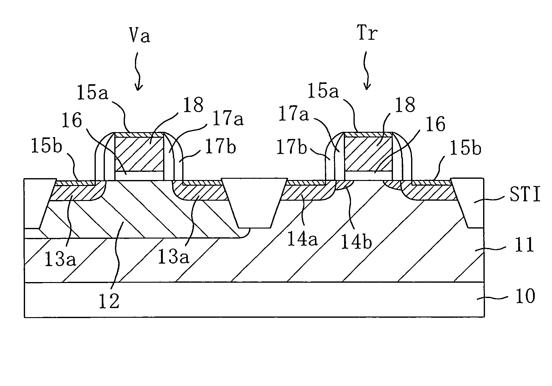
[0049]FIG. 1 is a cross-sectional view showing the structure of a semiconductor device according to a first embodiment in which a varactor (MIS capacitor) is combined with a CMOS device. The semiconductor device of this embodiment includes an STI (Shallow Trench Isolation) structure partitioning the surface of a semiconductor substrate 10 that is a Si substrate into a plurality of active regions. The plurality of active regions comprise transistor regions Tr to be formed with MISFETs of the CMOS device and varactor regions Va to be formed with varactors. Although the MISFETs of the CMOS device include an NMISFET and a PMISFET, this figure shows only a region of the semiconductor device to be formed with an NMISFET.

[0050] The semiconductor substrate 10 is formed with a P well region 11 doped with a P-type impurity and an N well region 12 obtained by doping a part of the P well region 11 with an N-type impurity. The N well region 12 shown in FIG. 1 is an active r...

embodiment 2

[0061] (Embodiment 2)

[0062]FIG. 3 is a cross-sectional view showing the structure of a semiconductor device according to a second embodiment in which a varactor (MIS capacitor) is combined with a CMOS device. The semiconductor device of this embodiment includes an STI (Shallow Trench Isolation) structure partitioning the surface of a semiconductor substrate 10 that is a Si substrate into a plurality of active regions. The plurality of active regions comprise transistor regions Tr to be formed with MISFETs of the CMOS device and varactor regions Va to be formed with varactors. Although the MISFETs of the CMOS device include an NMISFET and a PMISFET, this figure shows only a region of the semiconductor device to be formed with an NMISFET.

[0063] The semiconductor substrate 10 is formed with a P well region 11 doped with a P-type impurity and an N well region 12 obtained by doping a part of the P well region 11 with an N-type impurity. The N well region 12 shown in FIG. 3 is an active ...

embodiment 3

[0074] (Embodiment 3)

[0075]FIG. 5 is a cross sectional view showing the structure of a semiconductor device according to a third embodiment in which a varactor (MIS capacitor) is combined with a CMOS device. The semiconductor device of this embodiment includes an STI (Shallow Trench Isolation) structure partitioning the surface of a semiconductor substrate 10 that is a Si substrate into a plurality of active regions. The plurality of active regions comprise transistor regions Tr to be formed with MISFETs of the CMOS device and varactor regions Va to be formed with varactors. Although the MISFETs of the CMOS device include an NMISFET and a PMISFET, this figure shows only a region of the semiconductor device to be formed with an NMISFET.

[0076] The semiconductor substrate 10 is formed with a P well region 11 doped with a P-type impurity and an N well region 12 obtained by doping a part of the P well region 11 with an N-type impurity. The N well region 12 shown in FIG. 5 is an active r...


PUM


Abstract

A semiconductor device comprises varactor regions Va and transistor regions Tr. An active region for a varactor is formed with a substrate contact impurity diffusion region obtained by doping an N well region with N-type impurity at a relatively high concentration. However, any extension region (or LDD region) as in a varactor of a known semiconductor device is not formed in the active region for a varactor. On the other hand, parts of a P well region located to both sides of the polysilicon gate electrode in the transistor region Tr are formed with high-concentration source / drain regions and extension regions. Therefore, the extendable range of a depletion layer is kept wide to extend the capacitance variable range of the varactor.

Description

BACKGROUND OF THE INVENTION [0001] (1) Field of the Invention [0002] The present invention relates to a voltage-variable capacitor (varactor) used for a radio frequency (RF) circuit such as a voltage-controlled oscillator, and more particularly relates to a MIS capacitor fabricated using an existing CMOS process. [0003] (2) Description of Related Art [0004] Varactors that are voltage-variable capacitors have conventionally been widely used for many radio frequency (RF) circuits. One of known devices for realizing varactors is a device utilizing the depletion layer capacitance of a PN junction, more specifically a varactor diode. [0005] Tuning ratio (TR) representing the ratio between the capacitance C2 at a reverse bias voltage of zero and the capacitance C1 at a predetermined reverse bias voltage is often used as an index for evaluating performance of varactors. Larger tuning ratio (C2 / C1) allows significant change in the varactor capacitance even within the same gate voltage width...

Claims


Application Information

Patent Timeline
Patent Type & Authority Applications(United States)
IPC IPC(8): H01L27/04H01L21/265H01L21/336H01L21/822H01L21/8234H01L27/06H01L27/108H01L29/00H01L29/78H01L29/93H01L29/94
CPCH01L21/26586H01L27/0629H01L29/7833H01L29/6653H01L29/6659H01L29/665
Inventor KADOWAKI, TADASHIUMIMOTO, HIROYUKIHANDA, TAKATO
Owner GK BRIDGE 1
Why Eureka
Try Eureka