Flip-chip package

a technology of flip-chip and package, which is applied in the direction of semiconductor devices, semiconductor/solid-state device details, electrical devices, etc., can solve the problems of easy warpage or bump-breaking on the substrate, and achieve the effect of enhancing heat dissipation, eliminating the stress of flip-chip 220, and fine-pitch flip-chip mounting

Active Publication Date: 2005-03-03
ADVANCED SEMICON ENG INC
View PDF8 Cites 22 Cited by
  • Summary
  • Abstract
  • Description
  • Claims
  • Application Information

AI Technical Summary

Benefits of technology

[0017] In the second embodiment of the present invention, another flip-chip package 200 is illustrated in FIG. 4. The flip-chip package 200 comprises a semiconductor chip 220 and a composite chip carrier composed of a substrate 210 and a dummy die 230. The substrate 210 is a printed circuit board. The substrate 210 has a top surface 211, a bottom surface 212 and an opening 213 passing through the top surface 211 and the bottom surface 212. The dummy die 230 has a top surface with a redistribution layer 231 formed by the integrated circuit manufacturing process and a corresponding exposed bottom surface. A plurality of bumps 232 are formed on the top surface of the dummy die 230 and electrically connect the redistribution layer 231 for electrically connecting the substrate 210. A chip cavity of the chip carrier is formed by the top substrate of the dummy die 230 and the opening 213 of the substrate 210. The bottom surface of the dummy die 230 has a high thermal-conducting metal layer 233, such as gold

Problems solved by technology

Due to the different thermal expansion coefficient between the chip and the substrate, the flip-chip mounting region (i.e.

Method used


Image

  • Flip-chip package
  • Flip-chip package
  • Flip-chip package

Examples


first embodiment

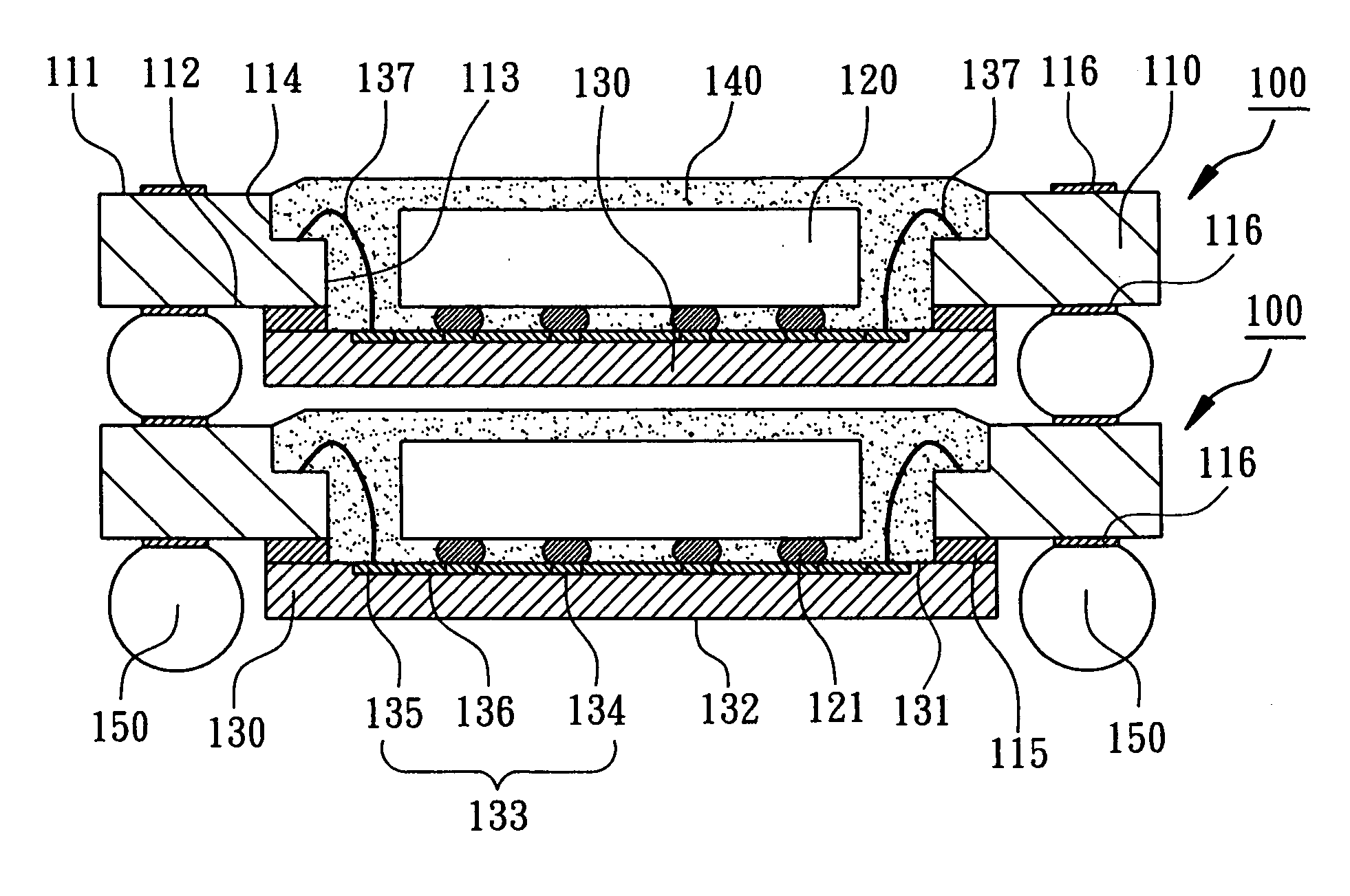
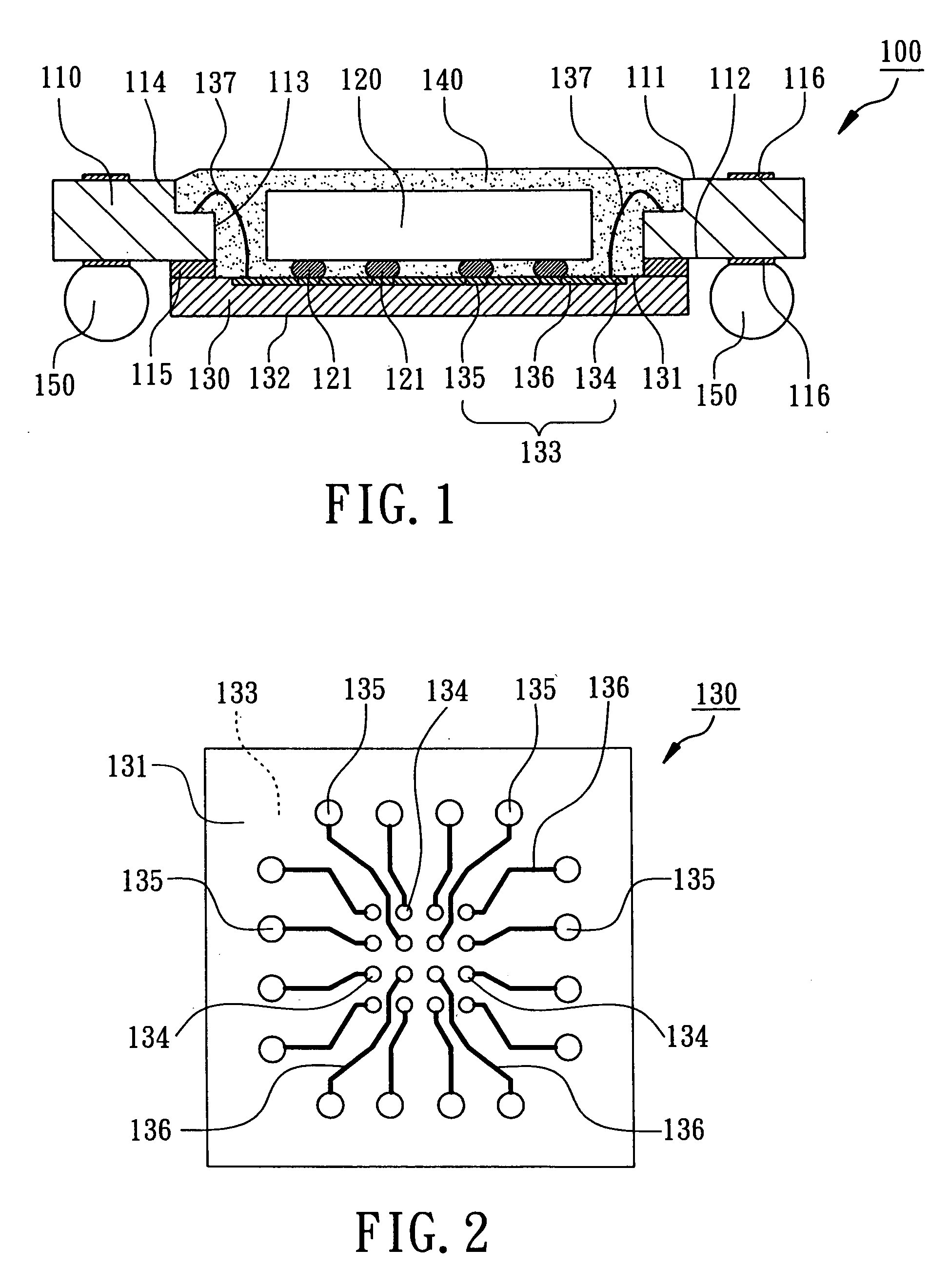
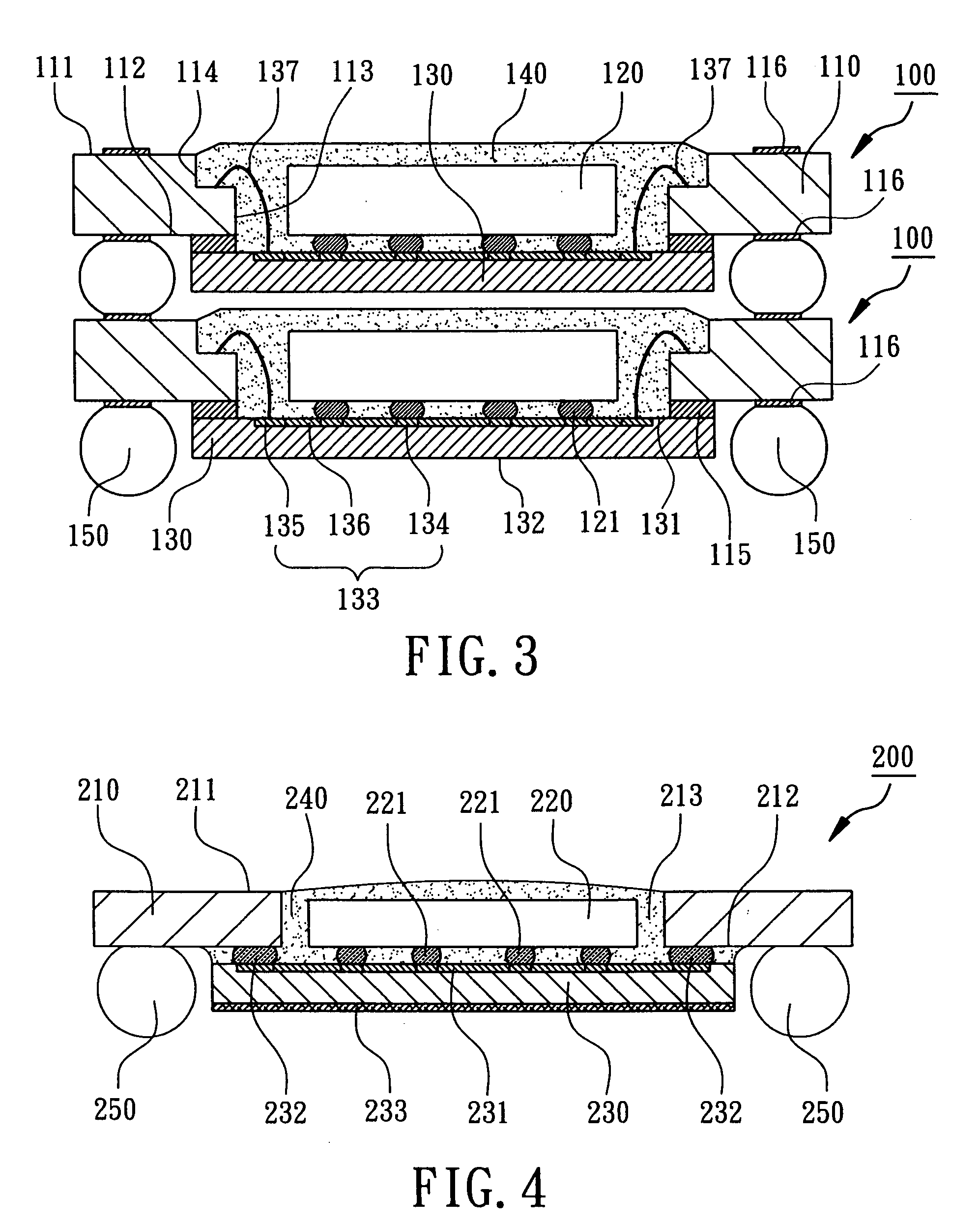
[0012] shown in FIG. 1, a flip-chip package 100 comprises a substrate 110, a chip 120, a dummy die 130 and a packaging body 140. The substrate 110 can be a printed circuit board made from BT resin, FR-4 resin or FR-5 resin. The substrate 110 possesses a top surface 111, a bottom surface 112 and an opening 113 passing through the top surface 111 and the bottom surface 112. It is preferable that the substrate 110 is a build-up multi-layer printed circuit board so as to have a stair 114 around the opening 113.

[0013] The dummy die 130 is disposed on the bottom surface 112 of the substrate 110 corresponding to the opening 113. In this embodiment, the dummy die 130 which thickness is about 200 μm (micro meter) has a surface 131 with a redistribution layer 133 (RDL) and a corresponding exposed surface 132. The surface 131 of the dummy die 130 is attached onto the bottom surface 112 of the substrate 110 by means of an adhesive tape 115 in order to form a composite chip carrier with a chip ...

second embodiment

[0017] In the present invention, another flip-chip package 200 is illustrated in FIG. 4. The flip-chip package 200 comprises a semiconductor chip 220 and a composite chip carrier composed of a substrate 210 and a dummy die 230. The substrate 210 is a printed circuit board. The substrate 210 has a top surface 211, a bottom surface 212 and an opening 213 passing through the top surface 211 and the bottom surface 212. The dummy die 230 has a top surface with a redistribution layer 231 formed by the integrated circuit manufacturing process and a corresponding exposed bottom surface. A plurality of bumps 232 are formed on the top surface of the dummy die 230 and electrically connect the redistribution layer 231 for electrically connecting the substrate 210. A chip cavity of the chip carrier is formed by the top substrate of the dummy die 230 and the opening 213 of the substrate 210. The bottom surface of the dummy die 230 has a high thermal-conducting metal layer 233, such as gold or cop...


PUM


Abstract

A flip-chip package comprises a substrate with an opening. A dummy die is disposed onto the substrate corresponding to the opening so as to form a composite chip carrier with a chip cavity. The dummy die has a redistribution layer which includes a plurality of flip-chip pads for flip-chip connection of a chip and a plurality of connecting pads around the dummy die for connecting the substrate. The dummy die mounts at least a chip by flip chip connection for being an electrical interface medium between the chip and the substrate in order to achieve thinner package thickness, high heat dissipation, fine pitch flip-chip mounting and eliminating flip-chip stress on the chip.

Description

FIELD OF THE INVENTION [0001] The present invention is generally relating to a flip-chip package, particularly to a flip-chip package comprising a chip carrier consisted of a dummy die and a substrate with an opening. BACKGROUND OF THE INVENTION [0002] In a conventional flip-chip package, a IC chip with a plurality of bumps is directly flip-chip mounted on a substrate, such as a printed circuit board or ceramic circuit board. A conventional flip-chip package had been brought up from R.O.C. (Republic Of China, Taiwan) Patent No. 457664 entitled “directly-downset flip-chip semiconductor package and its manufacturing process”. A chip is flip-chip mounted onto a substrate with a chip-cavity. The chip cavity of the substrate forms a plurality of dimple bonding pads for bonding the bumps of the chip. Due to the different thermal expansion coefficient between the chip and the substrate, the flip-chip mounting region (i.e. bumps) of the chip bears considerable thermal stress so that a warpa...

Claims


Application Information

Patent Timeline
IPC IPC(8): H01L23/24H01L23/498H01L25/10
CPCH01L23/24H01L2225/1058H01L25/105H01L2224/48091H01L2924/01079H01L2924/1433H01L23/49816H01L2225/1035H01L24/48H01L2924/01087H01L2224/16225H01L2924/19107H01L2924/3511H01L2225/1023H01L2924/00014H01L2924/14H01L2924/181H01L2224/4824H01L2224/73215H01L2924/00H01L2924/00012H01L2224/45099H01L2224/45015H01L2924/207
Inventor YANG, CHAUR-CHINWANG, SUNG-FEI
Owner ADVANCED SEMICON ENG INC
Why Eureka
Try Eureka