Voltage boosting circuit and method

a voltage boosting circuit and voltage boosting technology, applied in the direction of power conversion systems, dc-dc conversion, instruments, etc., can solve the problem of large power consumption

Active Publication Date: 2005-03-03
SAMSUNG ELECTRONICS CO LTD
View PDF1 Cites 97 Cited by
  • Summary
  • Abstract
  • Description
  • Claims
  • Application Information

AI Technical Summary

Benefits of technology

[0009] A boosting circuit is provided, having a small number of externally-mounted capacitors, which generates stepped-up and stepped-down boosted voltages through charging and pumping under two-phase driving, and a power supply unit for controlling the simultaneous output of a stepped-up voltage and a stepped-down voltage, an output of the stepped-up voltage, an output of the stepped-down voltage, and a cut-off of the output of the stepped-up voltage and the stepped-down voltage on the basis of a phase control signal generated from enable signals having logic states, which are changed in accordance with an amount of load, thereby minimizing its power consumption.

Problems solved by technology

In addition, because conventional power supply units comprising the conventional boosting circuit 100 output the boosted voltages without regard to the amount of load power there is a large amount of power consumption.

Method used


Image

  • Voltage boosting circuit and method
  • Voltage boosting circuit and method
  • Voltage boosting circuit and method

Examples


Embodiment Construction

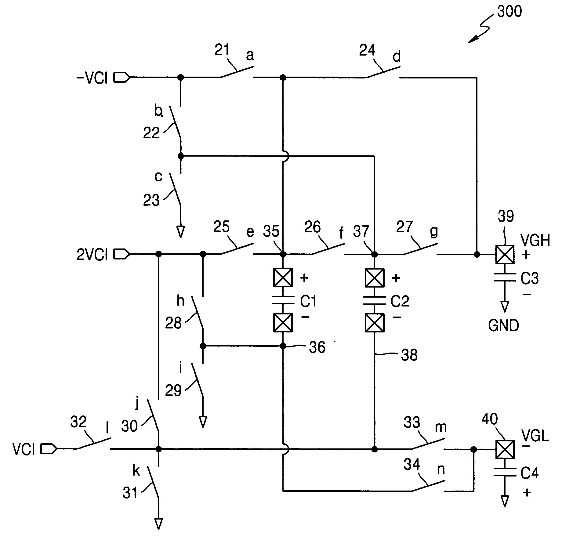
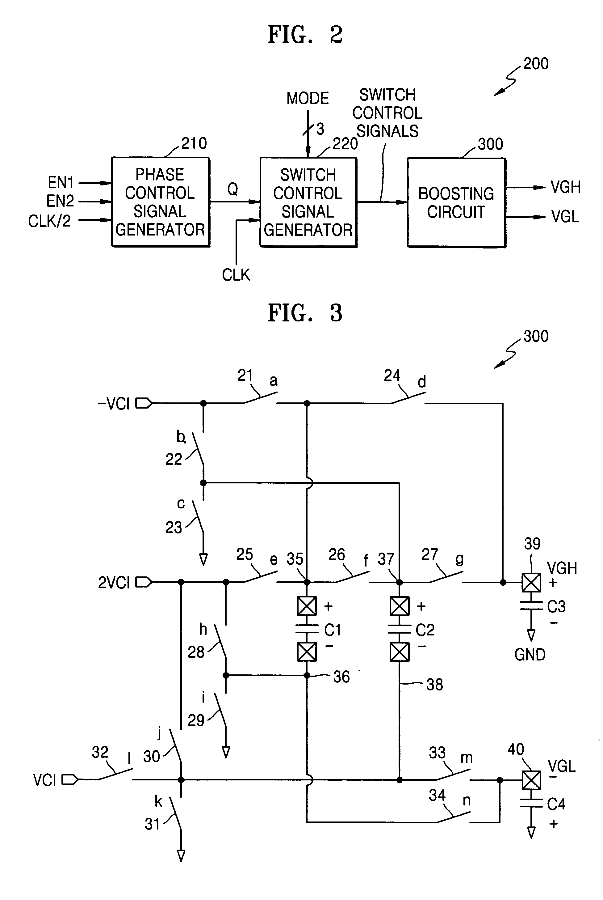
[0045]FIG. 2 is a block diagram of a boosting power supply unit 200 according to an exemplary embodiment of the present invention. Referring to FIG. 2, the boosting power supply unit 200 comprises a phase control signal generator 210, a switch control signal generator 220, and a boosting circuit 300.

[0046] The phase control signal generator 210 outputs a phase control signal Q having either a two phase pulse form or a logic state value form in response to each of four logic combinations of a first enable signal EN1 and a second enable signal EN2. A second clock signal CLK / 2 is used to generate the phase control signal Q. The second clock signal CLK / 2 is a clock signal obtained by dividing the frequency of a first clock signal CLK into two.

[0047] The switch control signal generator 220 generates and outputs two-phase step-down switch control signals corresponding to a mode signal MODE in a first logic state (for example, a low logic state) of the phase control signal Q, and generat...


PUM


Abstract

A voltage boosting circuit, boosting power supply unit and methods thereof are provided. A boosting power supply unit includes a boosting circuit having a small number of externally-mounted capacitors, which generates stepped-up and stepped-down boosted voltages through charging and pumping under two-phase control, so that the simultaneous output of the stepped-up voltage and the stepped-down voltage, the output of only the stepped-up voltage, the output of only the stepped-down voltage, and the cut-off of the output of the stepped-up voltage and the stepped-down voltage can be controlled on the basis of the phase control signal generated from the enable signals of which the logic states are changed in accordance with an amount of load.

Description

CROSS-REFERENCE TO RELATED APPLICATION [0001] This application claims priority to Korean Patent Application No. 2003-59094, filed on Aug. 26, 2003, in the Korean Intellectual Property Office, the disclosure of which is incorporated herein in its entirety by reference. BACKGROUND OF THE INVENTION [0002] 1. Technical Field [0003] The present invention relates to a power supply unit, and more specifically, to a boosting power supply unit and a power boosting control method. [0004] 2. Discussion of the Related Art [0005] In general, thin film transistors (TFTs) in liquid crystal panels having a turn on voltage of about 20V and a turn off voltage of about −20V are used to drive TFT liquid crystal display devices (LCDs), such as those for use with mobile video graphic adapters (VGA), etc. Such TFT turn-on / off voltages have slight deviations depending on the types of TFTs (for example, amorphous silicon (a-Si) TFTs, low-temperature polysilicon (LTPS) TFTs, continuous grain silicon (CGS) TF...

Claims


Application Information

Patent Timeline
Patent Type & Authority Applications(United States)
IPC IPC(8): H02M3/155H02M3/07
CPCH02M3/07H02M3/155
Inventor KIM, HYOUNG-RAE
Owner SAMSUNG ELECTRONICS CO LTD
Why Eureka
Try Eureka