Pattern recognition and metrology structure for an x-initiative layout design

a metrology structure and layout design technology, applied in the field of semiconductor processing, can solve problems such as the decrease of overall yield, and achieve the effect of facilitating the inspection of overlay accuracy

Inactive Publication Date: 2005-03-03
GLOBALFOUNDRIES INC
View PDF2 Cites 31 Cited by
  • Summary
  • Abstract
  • Description
  • Claims
  • Application Information

AI Technical Summary

Benefits of technology

Yet another aspect of the present invention employs diagonal (45 degree) lines in association with traditional hori

Problems solved by technology

Inaccuracies can cause a decrease in the overall yi

Method used


Image

  • Pattern recognition and metrology structure for an x-initiative layout design
  • Pattern recognition and metrology structure for an x-initiative layout design
  • Pattern recognition and metrology structure for an x-initiative layout design

Examples


Embodiment Construction

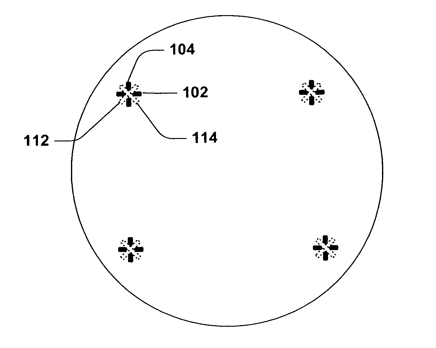
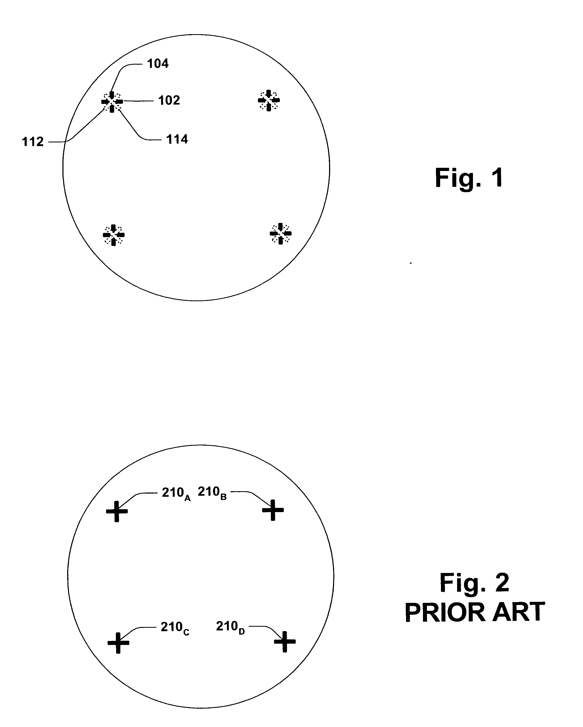
FIG. 1 illustrates an embodiment of the subject invention where two diagonal (45 degree) lines 112 and 114 are added to enhance the alignment of a semiconductor employing a design concurrent with the X-initiative. Lines 112 and 114 are utilized in conjunction with a traditional alignment mark drawn with two orthogonal lines 102 and 104 placed on a wafer 100. It is to be appreciated the lines 102, 104, 112 and 114 can be substantially similar in length, width and location relative to each other in all four locations shown.

In this particular embodiment, the two additional lines 112 and 114 lie at 45-degree angles to the original two lines employed for an alignment mark. The two additional lines are added as shown with substantially the same center as the original alignment marks. It should be appreciated that the addition of the two diagonal (45 degree) lines can be placed on at least the reticle and / or the wafer. It is to be understood that the centerline of the additional marks doe...


PUM


Abstract

The present invention relates to inspection methods and systems utilized to provide a best means for inspection of a wafer. The methods and systems include wafer-to-reticle alignment, layer-to-layer alignment and wafer surface feature inspection. The wafer-to-reticle alignment is improved by the addition of diagonal lines to existing alignment marks to decrease the intersection size and corresponding area that a desired point can reside. Layer-to-layer alignment is improved in a similar manner by the addition of oblique and/or non-linear line segments to existing overlay targets. Also, providing for wafer surface inspection in a multitude of desired diagonal axes allows for more accurate feature measurement.

Description

TECHNICAL FIELD The present invention generally relates to semiconductor processing, and in particular to improving wafer fabrication inspection by utilizing diagonal (45 degrees) lines in addition to traditional perpendicular lines of inspection, to manufacture improved semiconductor designs. BACKGROUND In the semiconductor industry, there is a continuing trend toward higher device densities. To achieve these high densities, there has been and continues to be efforts toward scaling down device dimensions (e.g., at submicron levels) on semiconductor wafers. In order to accomplish such high device packing density, smaller and smaller feature sizes are required in integrated circuits (ICs) fabricated on small rectangular portions of the wafer, commonly known as dies. This can include width and spacing of interconnecting lines, spacing and diameter of contact holes, surface geometry such as comers and edges of various features as well as surface geometry of other features. To scale d...

Claims


Application Information

Patent Timeline
IPC IPC(8): G03F7/20G03F9/00
CPCG03F7/70625Y10S438/975G03F9/7076G03F7/70633G03F7/20G03F9/00H01L21/20
Inventor PHAN, KHOI A.RANGARAJAN, BHARATHSINGH, BHANWAR
Owner GLOBALFOUNDRIES INC
Why Eureka
Try Eureka