

The use of a layout-optimization tool to increase the yield and reliability of VLSI designs
a layout optimization and design technology, applied in the direction of cad circuit design, program control, instruments, etc., can solve the problem that the attempt to do such layout modification by hand would be prohibitively expensiv
- Summary
- Abstract
- Description
- Claims
- Application Information
AI Technical Summary
Benefits of technology
Problems solved by technology
Method used
Image

Examples
Embodiment Construction
[0022] The present invention and the various features and advantageous details thereof are explained more fully with reference to the nonlimiting embodiments that are illustrated in the accompanying drawings and detailed in the following description. It should be noted that the features illustrated in the drawings are not necessarily drawn to scale. Descriptions of well-known components and processing techniques are omitted so as to not unnecessarily obscure the present invention in detail.
[0023] Specific embodiments of the invention will now be further described by the following, nonlimiting examples which will serve to illustrate in some detail various features of significance. The examples are intended merely to facilitate an understanding of ways in which the invention may be practiced and to further enable those of skill in the art to practice the invention. Accordingly, the examples should not be construed as limiting the scope of the invention.
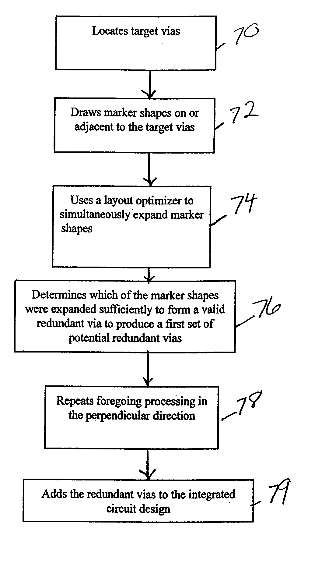
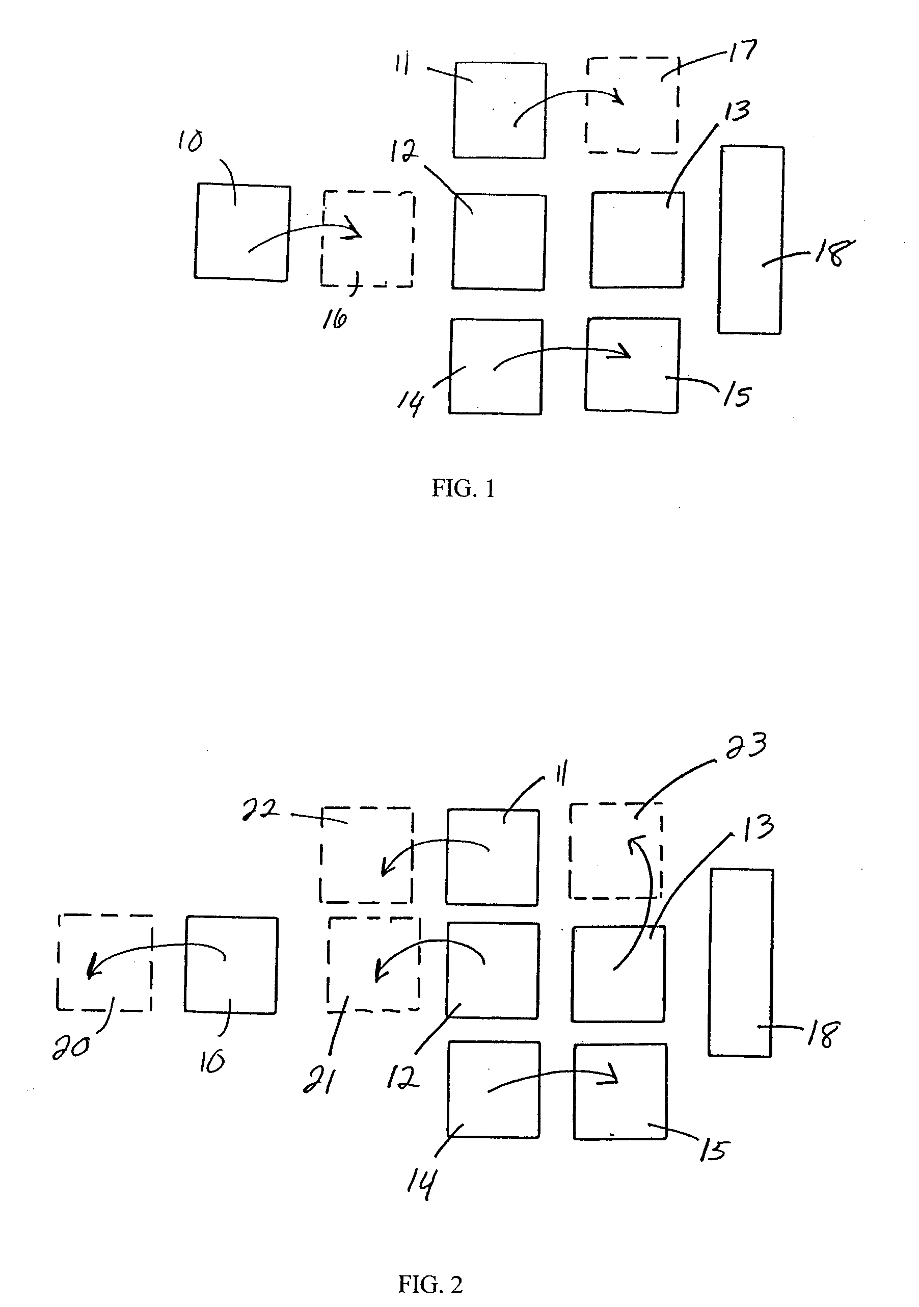
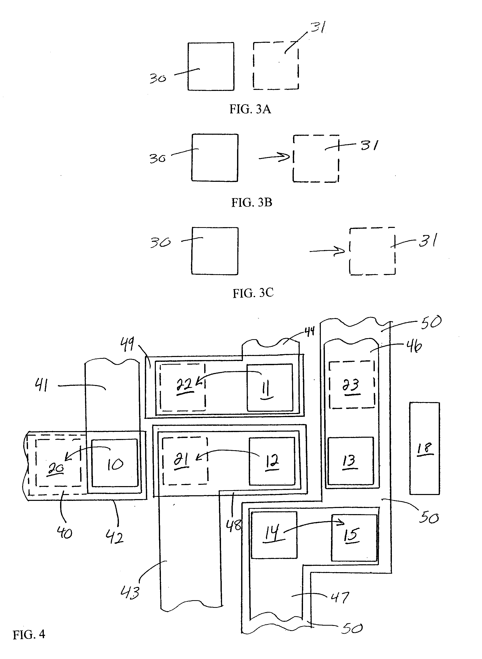
[0024] The invention optimizes...
PUM
 Abstract
Description
Claims
Application Information