
Apparatus and a manufacturing method of a thin-film transistor LCD

a thin-film transistor and manufacturing method technology, applied in the direction of electrical apparatus, semiconductor devices, transistors, etc., can solve the problems of high voltage, easy defects in the insulation layer, metal wiring etching phenomenon, etc., and achieve the effect of effective anti-electrostatic purpos

Inactive Publication Date: 2005-03-10
CHUNGHWA PICTURE TUBES LTD
View PDF0 Cites 4 Cited by
  • Summary
  • Abstract
  • Description
  • Claims
  • Application Information

AI Technical Summary

Benefits of technology

[0009] The main purpose of he present invention is to provide a thin-film transistor LCD (Light Crystal Display) apparatus. More particularly, it is a TFT-LCD apparatus comprising semiconductor layers. By using the semiconductor layer structure, it can overcome the light leakage problem of a TFT-LCD apparatus for achieving an effective light shielding purpose.
[0010] Another purpose of the present invention is to provide a TFT-LCD apparatus with an anti-electrostatic function. By using a semi-conductor layer structure, it can overcome signal-coupling problems between connecting wires for effectively achieving anti-electrostatic purpose.
[0011] Providing a TFT-LCD manufacturing method is another purpose of the present invention. More particularly, it relates to a TFT-LCD manufacturing method with a semi-conductor layer. By using this manufacturing method, it can include a semiconductor layer of TFT-LCD apparatus and the said semiconductor layer can effectively cover on the TFT-LCD apparatus for achieving an anti-electrostatic and light shielding purposes.

Problems solved by technology

This makes insulating layer easily occur defects in the gate electrode layer of a TFT-LCD apparatus.
Furthermore, the water vapor in the air etches into the panel, therefore, the gate driver IC inputs signals into the voltage of the wires and causes metal wiring etching phenomenon.
Especially, the input voltage is higher in the gate electrode and the metal wiring oxidation problem is occurred while using a gate electrode wire with AlNd.
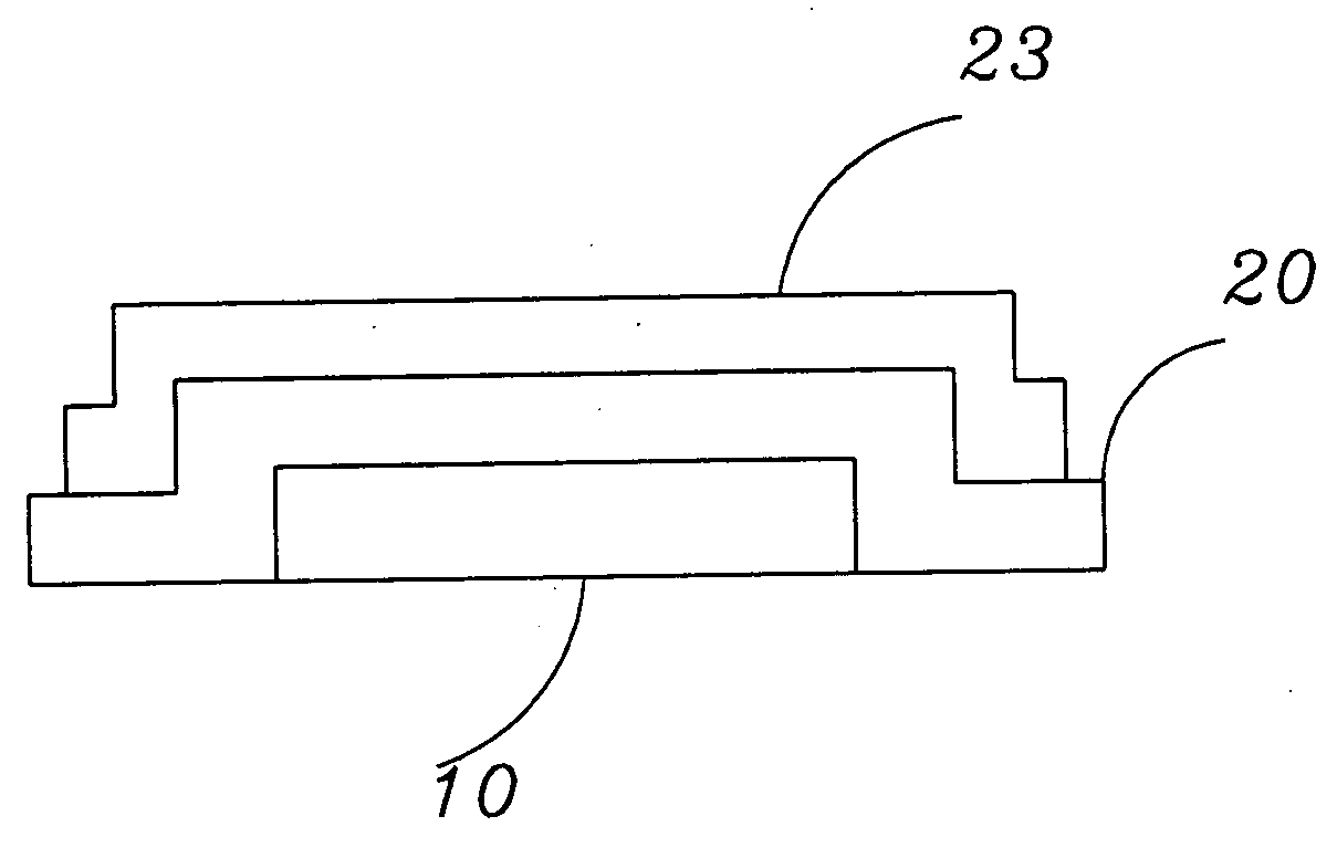
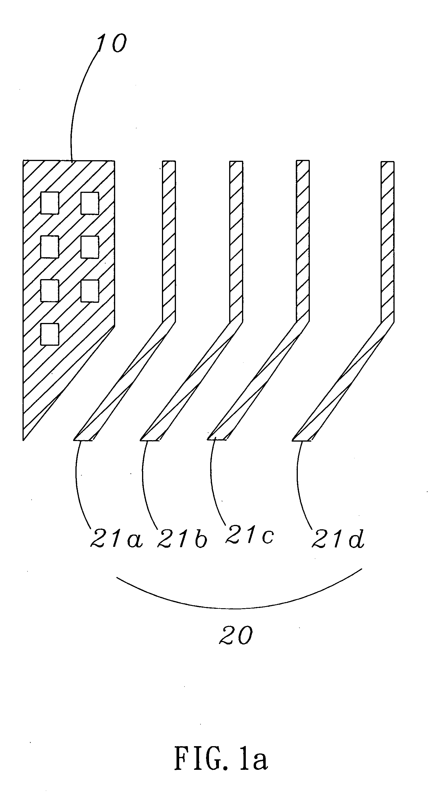
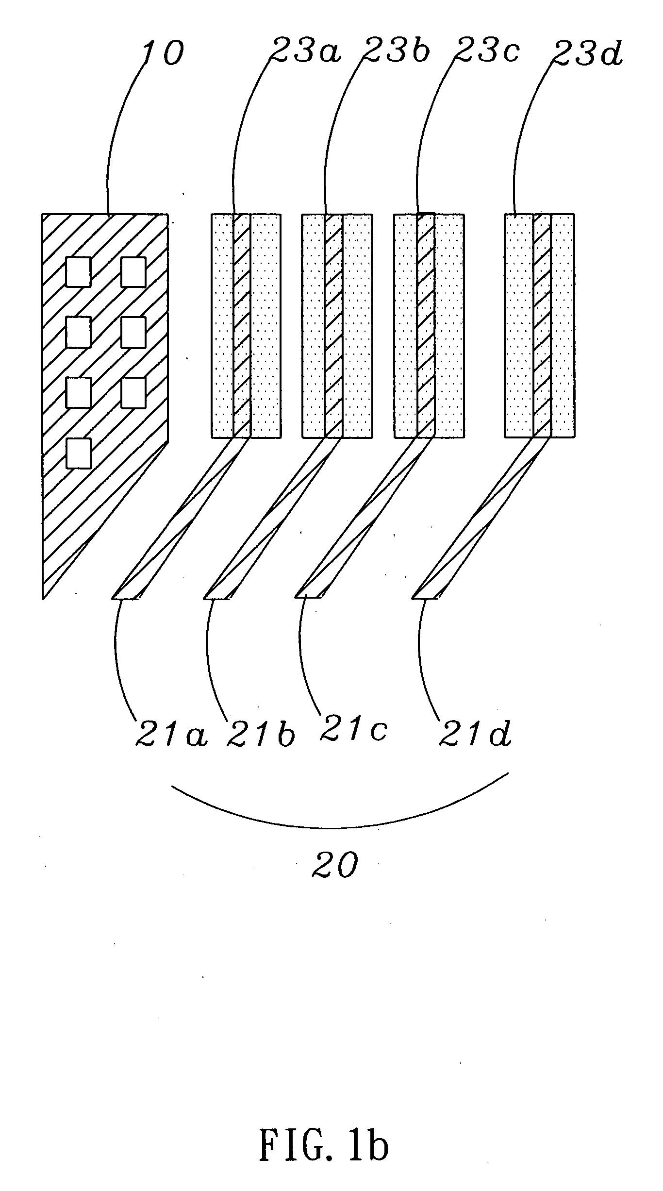
However, the width of the structure in said multiple metal passivation layers (23a, 23b, 23c, and 23d) is difficult to control, and causes wiring short-cut problems happen.
In addition, the coating method of said multiple metal passivation layers (23a, 23b, 23c, and 23d) enhances the wiring width become narrower, therefore, easily causes signal coupling problems as well as improper display.
Then, terminals in wiring area will be found while turning the light of the panel, especially the light leakage problem is occurred in the source electrode.
While the said color filter substrate (30) and multiple source electrode metal wires (41a, 41b, 41c, and 41d) without any passivation layers, the light-emitting problem is easily happened.
The said metal passivation layers can be a electrode metal passivation layer (42), however, the metal wiring width of the metal passivation layers is difficult to control as taking this solution.
Furthermore, incomplete light shielding and wiring shortcut is easily happened.
More, unnecessary noise and interference will occur in the signal coupling process.

Method used


Image

  • Apparatus and a manufacturing method of a thin-film transistor LCD
  • Apparatus and a manufacturing method of a thin-film transistor LCD
  • Apparatus and a manufacturing method of a thin-film transistor LCD

Examples


Embodiment Construction

[0023] The present invention relates to a TFT-LCD apparatus, which includes a substrate and the said substrate situated on the bottom side of the TFT-LCD apparatus. A first metal layer on the said substrate as a GE wire in the TFT-LCD apparatus is also included. Further, A semiconductor layer on the said first metal layer as an active layer in the apparatus is included. More, a second metal layer as a source electrode wire for effectively achieving back-light shielding and providing an anti-electrostatic protection is also included.

[0024] Next, as shown in FIG. 3a, it is a cross-sectional view showing a gate electrode fully covered with a semiconductor layer structure according to the present invention. The said TFT-LCD apparatus includes a TFT substrate (10), and the top of the said TFT substrate (10) has at least one metal layer (80). The said metal layer (80) has multiple metal wires (81a, 81b, 81c, and 81d) situated on the top side of the said TFT substrate (10). At least one s...


PUM


Abstract

A thin-film transistor (hereinafter referred to as “TFT”) LCD (liquid crystal display) apparatus and its manufacturing method can improve the shortages of improper metal coating protection and incomplete light shielding. Besides, the semi-conductor layer usually uses A-Si layer as a light shielding and a coating materials. Furthermore, the TFT-LCD apparatus and its manufacturing method of the present invention can effectively overcome incomplete light shielding problem of the prior art without using extra numbers of masks for achieving the anti-electrostatic purpose.

Description

BACKGROUND OF THE INVENTION [0001] 1. Filed of the Invention [0002] The present invention relates to a TFT-LCD apparatus. More particularly, it means a TFT-LCD apparatus with a semiconductor passivation layer. By using a TFT-LCD apparatus of the present invention can effectively overcome the incomplete light-shielding problem and further achieve the anti-electrostatic purpose. [0003] 2. Description of the Related Art [0004] In the traditional TFT-LCD apparatus, the residual stress is formed after completing panel cutting manufacturing process. This makes insulating layer easily occur defects in the gate electrode layer of a TFT-LCD apparatus. Furthermore, the water vapor in the air etches into the panel, therefore, the gate driver IC inputs signals into the voltage of the wires and causes metal wiring etching phenomenon. Especially, the input voltage is higher in the gate electrode and the metal wiring oxidation problem is occurred while using a gate electrode wire with AlNd. [0005]...

Claims


Application Information

Patent Timeline
Patent Type & Authority Applications(United States)
IPC IPC(8): H01L29/786
CPCH01L29/78633H01L29/78606
Inventor LIOU, MENG-CHICHANG, YANG-HUILIN, KUANG-HSIANG
Owner CHUNGHWA PICTURE TUBES LTD
Learn More