Thin film resonator, method for making thin film resonator and filter having thin film resonators
- Summary
- Abstract
- Description
- Claims
- Application Information
AI Technical Summary
Benefits of technology
Problems solved by technology
Method used
Image
Examples
first embodiment
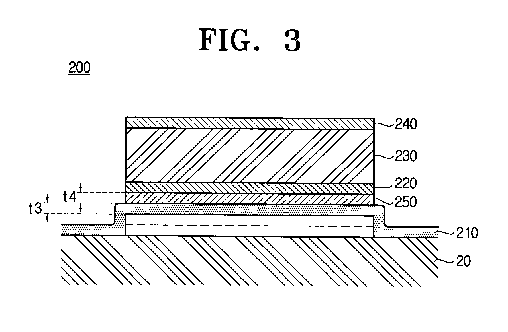
[0038]FIG. 3 is a cross-sectional view of a thin film resonator according to the present invention. As shown in FIG. 3, a thin film resonator 200 comprises a membrane layer 210, a mass loading layer 250, a lower electrode 220, a piezoelectric layer 230 and an upper electrode 240. Since the piezoelectric layer 230 and the upper electrode 240 are identical to those used in a conventional thin film resonator, a detailed explanation thereof will be omitted.
[0039] According to the first embodiment, the thin film resonator 200 interposes the mass loading layer 250 between the lower electrode 220 and the membrane layer 210. The resonant frequency of the thin film resonator 200 can be adjusted according to the thickness of the mass loading layer 250.
[0040] The membrane layer 210 is deposited on a substrate 20 to vibratably support the thin film resonator 200 on the substrate 20. The membrane layer 210 vibrates in combination with the vibration of the piezoelectric layer 230. The membrane l...
second embodiment
[0042]FIG. 5 is a cross-sectional view showing the structure of a thin film resonator according to the present invention. As shown in FIG. 5, the thin film resonator 200 is characterized in that both the top and bottom of the lower electrode 220 are surrounded by the membrane layer 215. To be specific, the lower electrode 220, made of a metallic material having a greater Young's Modulus, is disposed within a membrane layer 215 made of a material having a smaller Young's Modulus, such as silicon dioxide. The overall rigidity of the membrane layer 215 is thus improved, which consequently prevents distortion of the membrane layer 215 and improves the stability and reliability of the membrane layer 215. Also, the membrane layer 215 can absorb chemical and mechanical impacts that have caused problems in the prior art, and enables free selection of a material for the lower electrode 220, thereby reducing the manufacturing cost and simplifying the process of manufacturing the thin film res...
third embodiment
[0043]FIG. 6 shows the structure of a thin film resonator 200 according to the present invention. The thin film resonator 200 includes a membrane layer 213, a mass loading layer 250, a lower electrode 220, a piezoelectric layer 230 and an upper electrode 240. The lower surface of the mass loading layer 250 and the upper surface of the lower electrode 220 are surrounded by the membrane layer 213. Accordingly, the lower electrode 220 and the mass loading layer 250 can be selected from a wide range of materials. Also, the resonant frequency can be more easily adjusted by the addition of the mass loading layer 250.
[0044] Hereinafter, a method for manufacturing a thin film resonator according to the present invention, and particularly the third embodiment, will be explained in detail with reference to the accompanying drawings.
[0045] As shown in FIG. 7A, a sacrificial layer 290 is first formed on a substrate 20 and then patterned by a predetermined etching process, for example, photolit...
PUM
 Abstract
Description
Claims
Application Information


