A design method of lithographic overlay marking

A design method and lithographic overlay technology, which are applied in optics, instruments, and photoplate-making processes on patterned surfaces, etc., can solve problems such as the inability to meet the compensation needs of lithography processes, and the inability to use high-order error compensation algorithms, etc., to achieve reflection Effects of process manufacturing error, improvement of chip manufacturing yield, improvement of feedback correction accuracy and overlay error compensation accuracy

Active Publication Date: 2021-11-26
NANJING CHENGXIN INTEGRATED CIRCUIT TECH RES INST CO LTD
View PDF5 Cites 0 Cited by
  • Summary
  • Abstract
  • Description
  • Claims
  • Application Information

AI Technical Summary

Problems solved by technology

For example, lithography equipment manufacturers suggest that the second-order overlay error compensation algorithm requires no less than 8 exposure area data points; the third-order overlay error compensation algorithm requires no less than 12 exposure area data points, Therefore, from Figure 4 It can be seen that the existing overlay mark layout in the paper cannot meet the compensation needs of the actual lithography process
[0005] In addition, in the traditional process measurement process, the overlay mark measurement of different exposure areas in the wafer is often limited to Figure 4 5 data points shown, and using the linear overlay error compensation method
When the residual error after overlay error compensation is still outside the specified range value, the data will not be available for use with higher order error compensation algorithms

Method used


Image

  • A design method of lithographic overlay marking
  • A design method of lithographic overlay marking
  • A design method of lithographic overlay marking

Examples


Embodiment

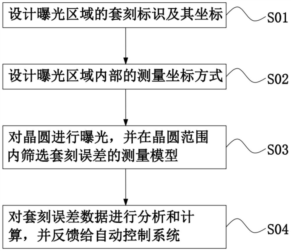
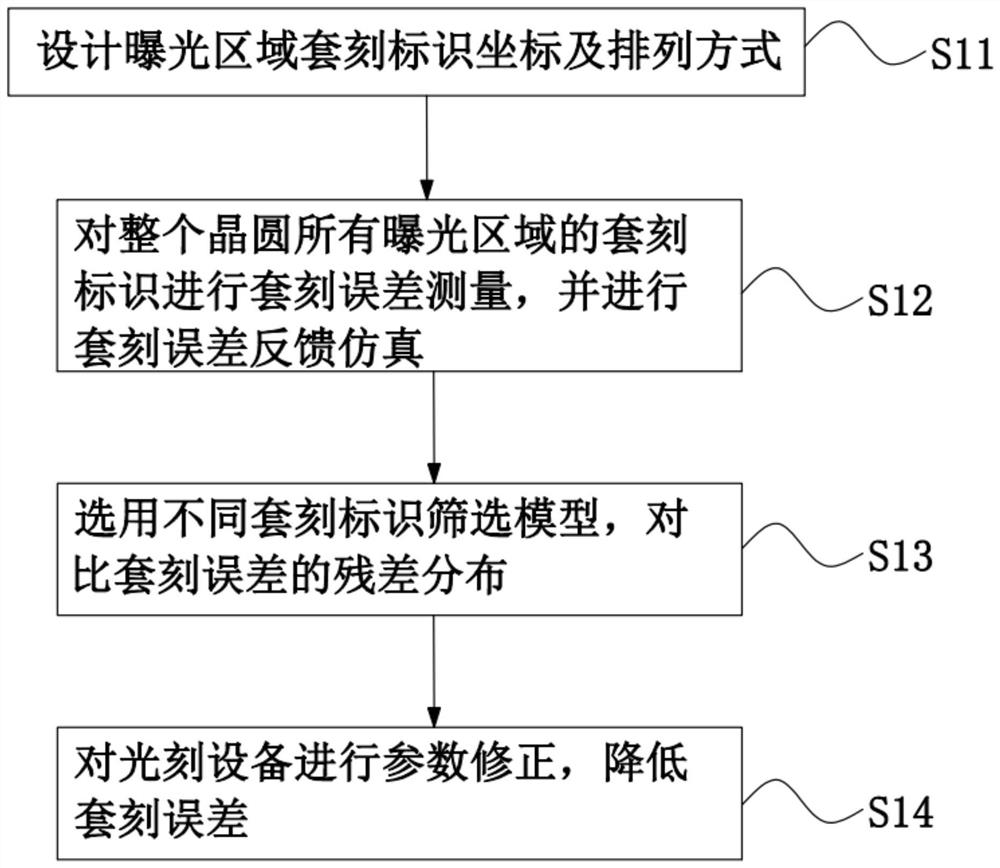
[0035] A method for designing a photolithographic overlay mark, comprising the steps of:

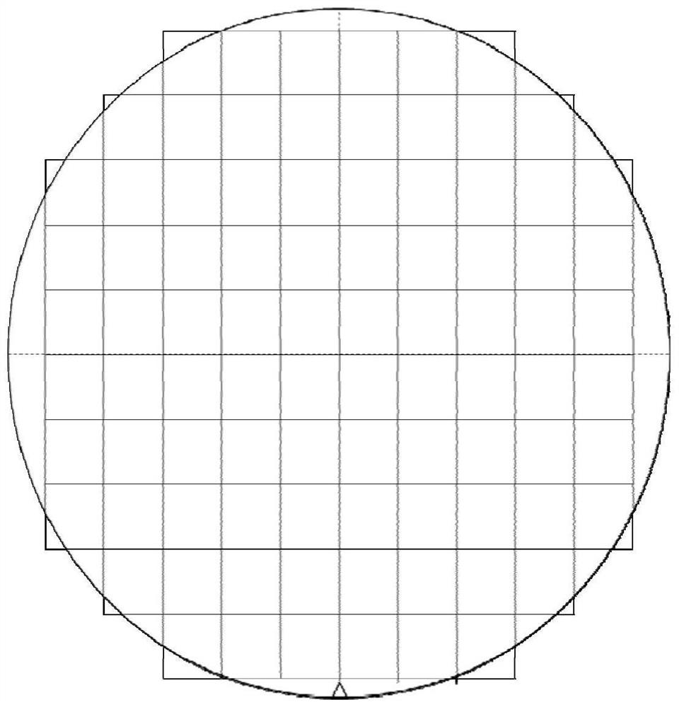
[0036] S01. Design the overlay marks and their coordinates inside the exposure area. There are no less than 10 overlay marks in each exposure area, and the coordinate design of the overlay marks evenly covers the entire exposure area;

[0037] S02. Design the measurement coordinate method inside the exposure area, and measure the coordinates through two design methods: the complementary point selection method and the comprehensive point selection method;

[0038] S03. Expose the wafer, and screen the measurement model of the overlay error within the wafer range. In the wafer coordinate system, mark all the exposure areas according to the horizontal and vertical directions, and optimize the exposure area according to the actual process characteristics. Carry out overlay error measurement;

[0039] S04. Analyze and calculate the overlay error data, and feed it back to the automatic contro...


PUM


Abstract

A photolithographic overlay mark design method of the present invention relates to the technical field of integrated circuit technology application, including step S01, designing the overlay mark and its coordinates inside the exposure area, and the overlay mark in each exposure area is not less than 10 First, the coordinate design of the overlay mark evenly covers the entire exposure area; S02, design the measurement coordinate method inside the exposure area, and measure the coordinates through two design methods: the complementary point selection method and the comprehensive point selection method; S03, carry out the process on the wafer Expose, and screen the overlay error measurement model within the wafer range, and label all exposure areas in the horizontal and vertical directions in the wafer coordinate system; S04, analyze and calculate the overlay error data, and feed back to The automatic control system is used to automatically correct the parameters of the lithography equipment, which improves the flexibility of measurement and the reliability of data, and improves the accuracy of feedback correction and overlay error compensation.

Description

technical field [0001] The invention relates to the technical field of integrated circuit technology application, in particular to a method for designing a photolithographic overlay mark. Background technique [0002] In the field of integrated circuit technology, due to the extremely complex process, it is particularly important and difficult to ensure precise alignment between layers to have a very small overlay error. [0003] Integrated circuit engraving and feedback problems are important factors that plague device yield. According to the method of feedback correction, the problem of overlay error feedback is divided into overlay error correction within exposure patterns and overlay error correction between exposure patterns. The overlay error correction within the exposure pattern refers to the correction of the overlay error inside each exposure area. It is realized by measuring the overlay error at the edge and inside of each exposure field and using a linear or hig...

Claims


Application Information

Patent Timeline
Patent Type & Authority Patents(China)
IPC IPC(8): G03F9/00
CPCG03F9/7003G03F9/7046G03F9/7088
Inventor 张利斌韦亚一董立松粟雅娟
Owner NANJING CHENGXIN INTEGRATED CIRCUIT TECH RES INST CO LTD
Why Eureka
Try Eureka