Wiring board and multilayer wiring board

a multi-layer wiring board and wiring board technology, applied in the direction of metallic pattern materials, electrography/magnetography, synthetic resin layered products, etc., can solve the problems of long mask production period, considerable cost of multi-layer wiring board manufacturing, and special mask production

Inactive Publication Date: 2005-03-10
KK TOSHIBA
View PDF11 Cites 20 Cited by
  • Summary
  • Abstract
  • Description
  • Claims
  • Application Information

AI Technical Summary

Problems solved by technology

This screen printing system, however, requires preparation-of a dedicated mask corresponding to each circuit pattern, bringing about a problem that multilayer wiring boards, in particular, which are likely to be put into diversified small-quantity production require many kinds of dedicated masks, resulting in longer period for producing the masks as well as considerable cost for manufacturing the multilayer wiring boards.
There is another problem that a dedicated mask needs to be produced again even for a partial change in the circuit pattern, failing to take flexible response to such a change.
With such an electrophotographic system, however, it is impossible in principle to impart an electrification property to the conductive metal particles attached to the surface of the insulating resin.
Further, in this electrophotographic system, it is possible to impart the electrification property to them if the surface of the insulating resin is formed of a metal oxide film, but the formation of a highly-precise conductive circuit pattern has been difficult due to extreme difficulty in adjusting the thickness and quality of the oxide film and controlling the quantity of electric charges.
As described above, in forming the conductive circuit pattern using the electrophotographic system, conductivity and imparting of the electrification property are in a trade-off relation, which has posed such a problem that it is difficult to obtain predetermined conductivity while keeping the electrification property.
Especially, in order to form a microscopic pattern such as a circuit pattern with high precision, controlling the electrification property is extremely important, but the industrial production of a conductive resin layer which can achieve both high precision in circuit formation and good electric characteristics has been extremely difficult.

Method used


Image

  • Wiring board and multilayer wiring board
  • Wiring board and multilayer wiring board
  • Wiring board and multilayer wiring board

Examples


first embodiment

[0027] (First Embodiment)

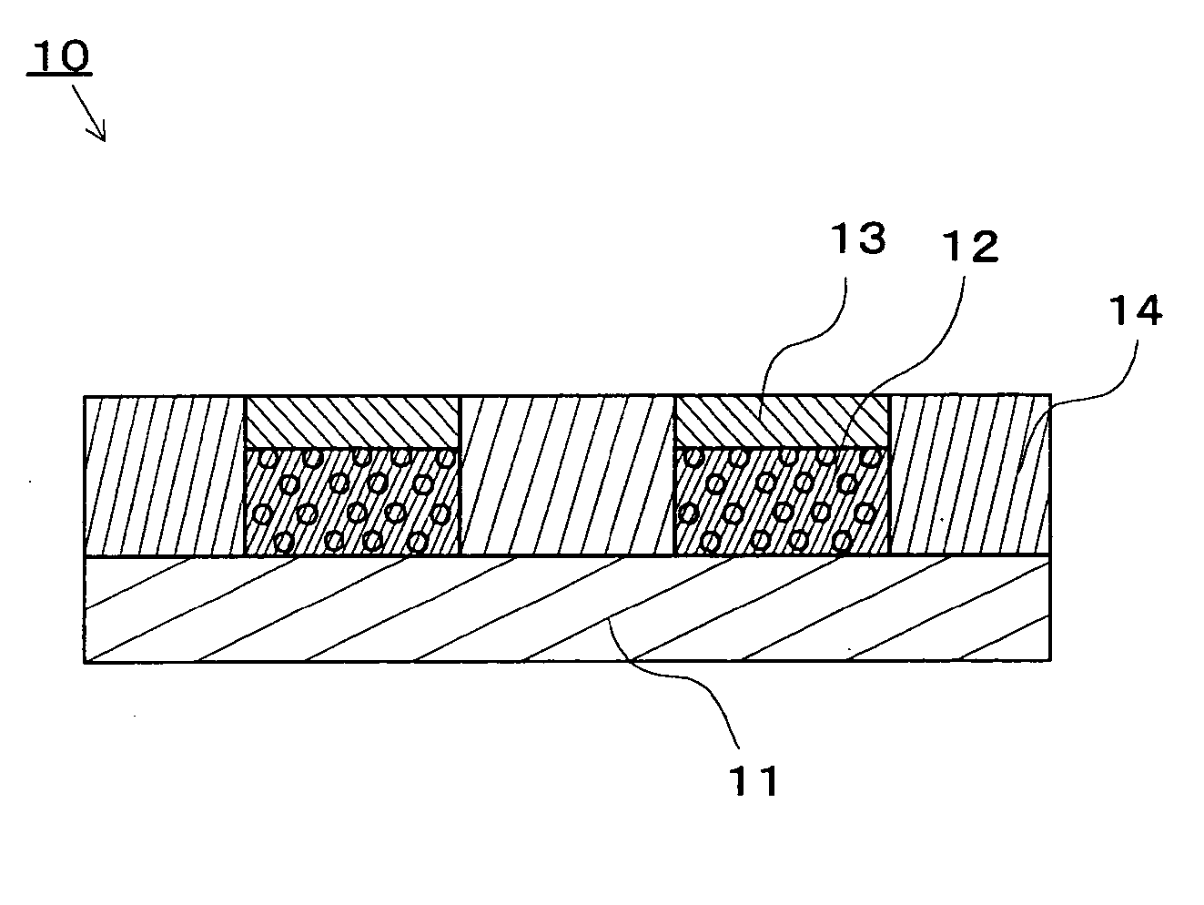
[0028]FIG. 1 schematically shows a cross-sectional view of a wiring board 10 composed of a single layer of the first embodiment of the present invention.

[0029] The wiring board 10 is composed of a base material 11, a nonconductive metal-containing resin layer 12 selectively formed on the base material 11, a conductive conductor metal layer 13 formed on the metal-containing resin layer 12, and a resin layer 14 selectively formed on the base material 11.

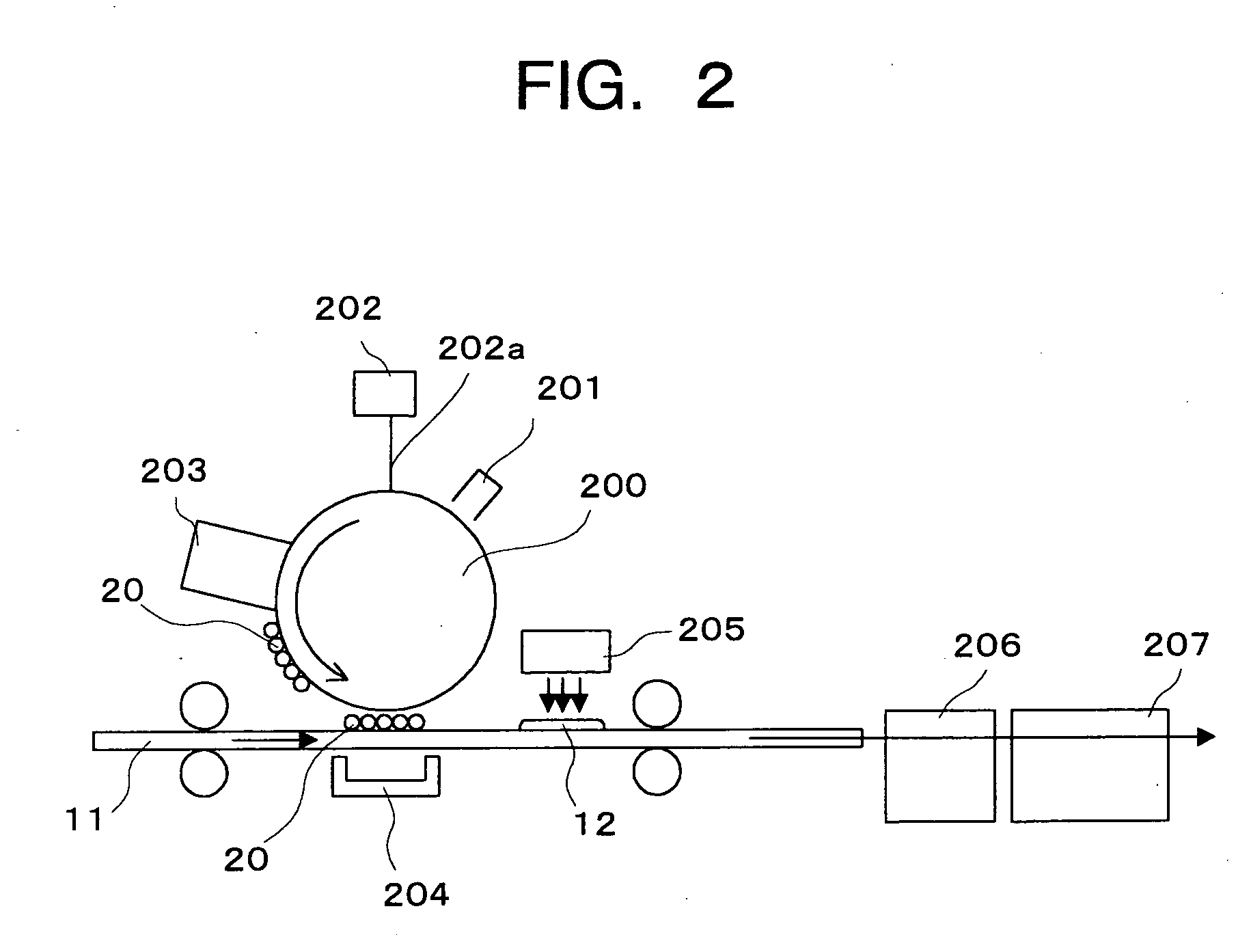
[0030] An example of the forming process of the wiring board 10 will be described with reference to FIG. 2 and FIG. 3.

[0031]FIG. 2 is a view schematically showing the forming process of a conductor pattern of the first embodiment of the present invention. FIG. 3 is a view schematically showing the forming process of an insulating pattern of the first embodiment. Further, FIG. 4 shows a cross-sectional view schematically showing a metal-containing resin particle 20 forming the nonconductive metal-containing r...

second embodiment

[0065] (Second Embodiment)

[0066]FIG. 6 shows a cross-sectional view of a multilayer wiring board 30 of a second embodiment formed by alternating-the above-described conductor pattern forming process and insulating pattern forming process. Note that the same reference numerals are assigned to the same portions as those in the configuration of the wiring board 10 of the first embodiment and the explanation thereof will be omitted. The multilayer wiring board 30 of the second embodiment is formed by the electrophotographic system in the similar manner to the wiring board 10 of the first embodiment.

[0067] A first layer constituting the multilayer wiring board shown in FIG. 6 is composed of a base material 31, a nonconductive metal-containing resin layer 32 selectively formed on the base material 31, a conductive conductor metal layer 33 formed on the metal-containing resin layer 32, a resin layer 34 selectively formed on the base material 31 and the conductor metal layer 33, and a via ...

third embodiment

[0092] (Third Embodiment)

[0093]FIG. 10 shows a cross-sectional view of a multilayer wiring board 50 of a third embodiment formed by alternating the above-described conductor pattern forming process and insulating pattern forming process. Note that the same reference numerals are assigned to the same portions as those in the configuration of the first and second embodiments and repeated explanation thereof will be omitted. The multilayer wiring board 50 of the third embodiment is formed by the electrophotographic system as in the first and second embodiments.

[0094] The multilayer wiring board 50 shown in FIG. 10 includes a base material 51 having at least one through hole 57 opened, nonconductive metal-containing resin layers 52 selectively formed on the front and rear faces of the base material 51, conductive conductor metal layers 53 formed on the metal-containing resin layers 52, and a conductor portion 54 provided in the through hole 57 which electrically connects the respective...


PUM

PropertyMeasurementUnit
diameteraaaaaaaaaa
diameteraaaaaaaaaa
diameteraaaaaaaaaa

Abstract

A wiring board formed by an electrophotographic system of transferring a visible image to a substrate, the wiring board including: a substrate to which a visible image is transferred; a nonconductive metal-containing resin layer selectively formed on the substrate and containing metal particulates dispersed therein; a conductive conductor metal layer formed on the metal-containing resin layer; and a resin layer formed contiguously to the metal-containing resin layer on the substrate.

Description

CROSSREFERENCE TO RELATED APPLICATIONS [0001] This application is based upon and claims the benefit of priority from the prior Japanese Patent Application No. 2003-280699, filed on Jul. 28, 2003; the entire contents of which are incorporated herein by reference. BACKGROUND [0002] 1. Field of the Invention [0003] The present invention relates to a wiring board and a multilayer wiring board formed by an electrophotographic system. [0004] 2. Description of the Related Art [0005] Conventionally, a screen printing system has been in wide use as a method for forming a circuit pattern on a substrate constituting a wiring board and a multilayer wiring board. This screen printing system applies a paste on the substrate in a predetermined circuit pattern, the paste being made by mixing metal powder of silver (Ag), platinum (Pt), copper (Cu), palladium (Pd) or the like with a binder such as ethyl cellulose and adjusting the viscosity of the resultant mixture using a solvent such as terpineol, ...

Claims


Application Information

Patent Timeline
Patent Type & Authority Applications(United States)
IPC IPC(8): C23C18/16B32B3/00B32B15/08B32B27/06B32B27/18C25D7/00H05K1/09H05K3/10H05K3/12H05K3/18H05K3/24H05K3/42H05K3/46
CPCB32B27/06B32B27/18H05K3/1266H05K3/246H05K3/428Y10T428/24917H05K3/4664H05K2201/0215H05K2201/0347H05K2203/0517H05K3/4647G03G15/224G03G15/6585G03G15/6591H05K1/09H05K3/12
Inventor AOKI, HIDEOYAMAGUCHI, NAOKOTAKUBO, CHIAKI
Owner KK TOSHIBA
Why Eureka
Try Eureka