Active matrix substrate and display device comprising same

Active Publication Date: 2005-03-17
SHARP KK
View PDF12 Cites 51 Cited by
  • Summary
  • Abstract
  • Description
  • Claims
  • Application Information

AI Technical Summary

Benefits of technology

[0028] The present invention is made in view of the foregoing conventional problems, and the present invention provides an active matrix substrate in which unevenness in the gate-drain capacitances cgd among the TFTs can be prevented even when a size and/or a shape of

Problems solved by technology

Unlike a conventional photolithography method, the ink jet printing possibly causes not only the problem of misalignment of the electrode layers, but also such a problem that sizes and/or shapes of patterns thereof become different (deviated) from what they are supposed to be (from its designed value), due to miss-shot of the droplets (the droplets are inaccurately shot and land off of a predetermined positions of the TFTs), which causes unevenness among the droplets in terms of their shapes.
For example, when the ink jet printing is carried out to form a resist p

Method used


Image

  • Active matrix substrate and display device comprising same
  • Active matrix substrate and display device comprising same
  • Active matrix substrate and display device comprising same

Examples


Embodiment Construction

[0053] The following description deals with one embodiment of the present invention with reference to figures.

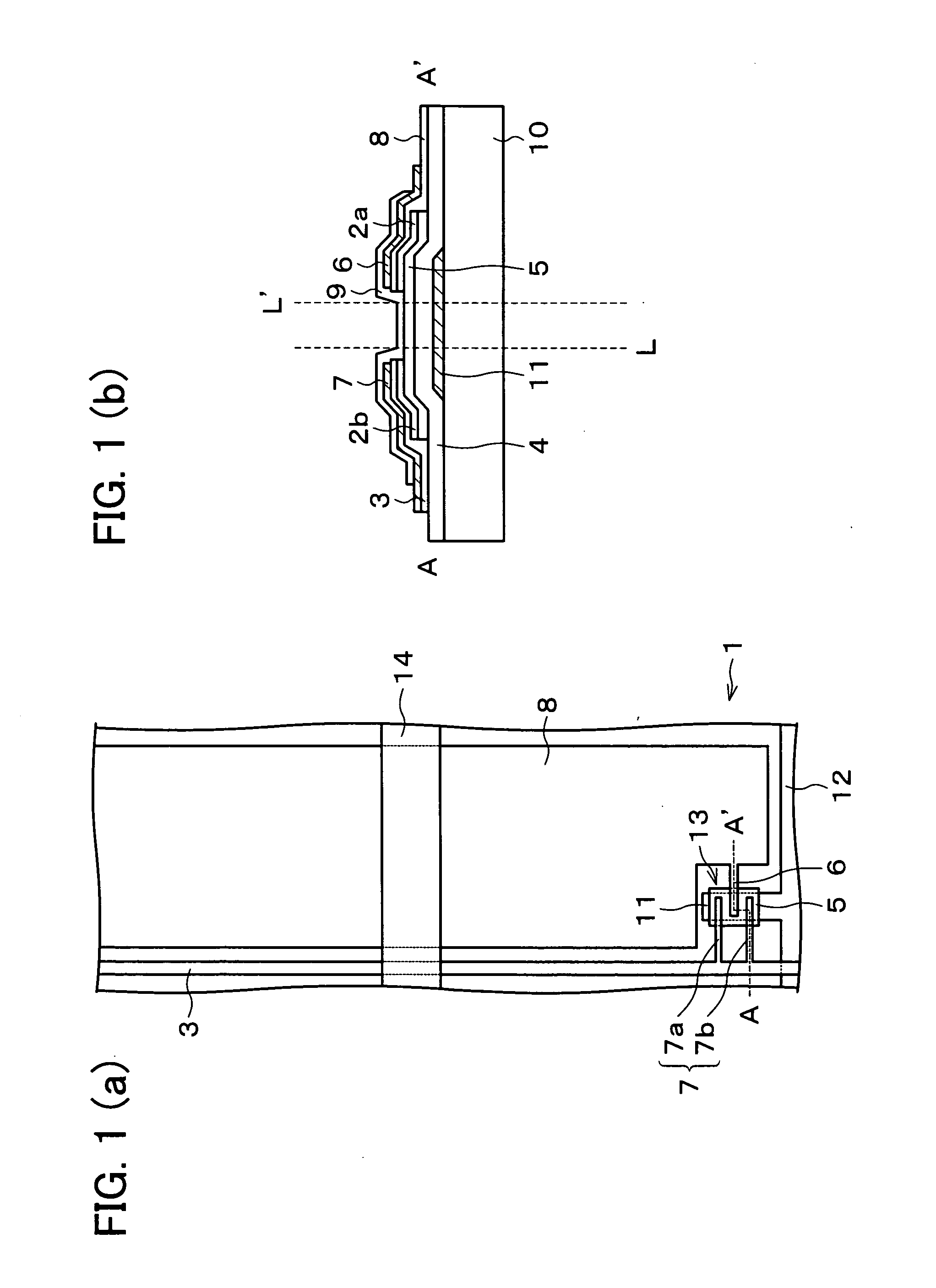
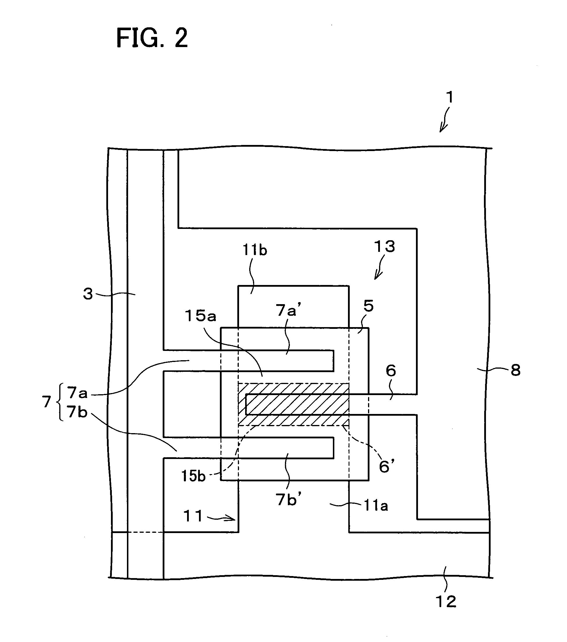
[0054] Firstly, in the present embodiment, a method for manufacturing an active matrix substrate is described with reference to FIGS. 1(a) and 1(b).

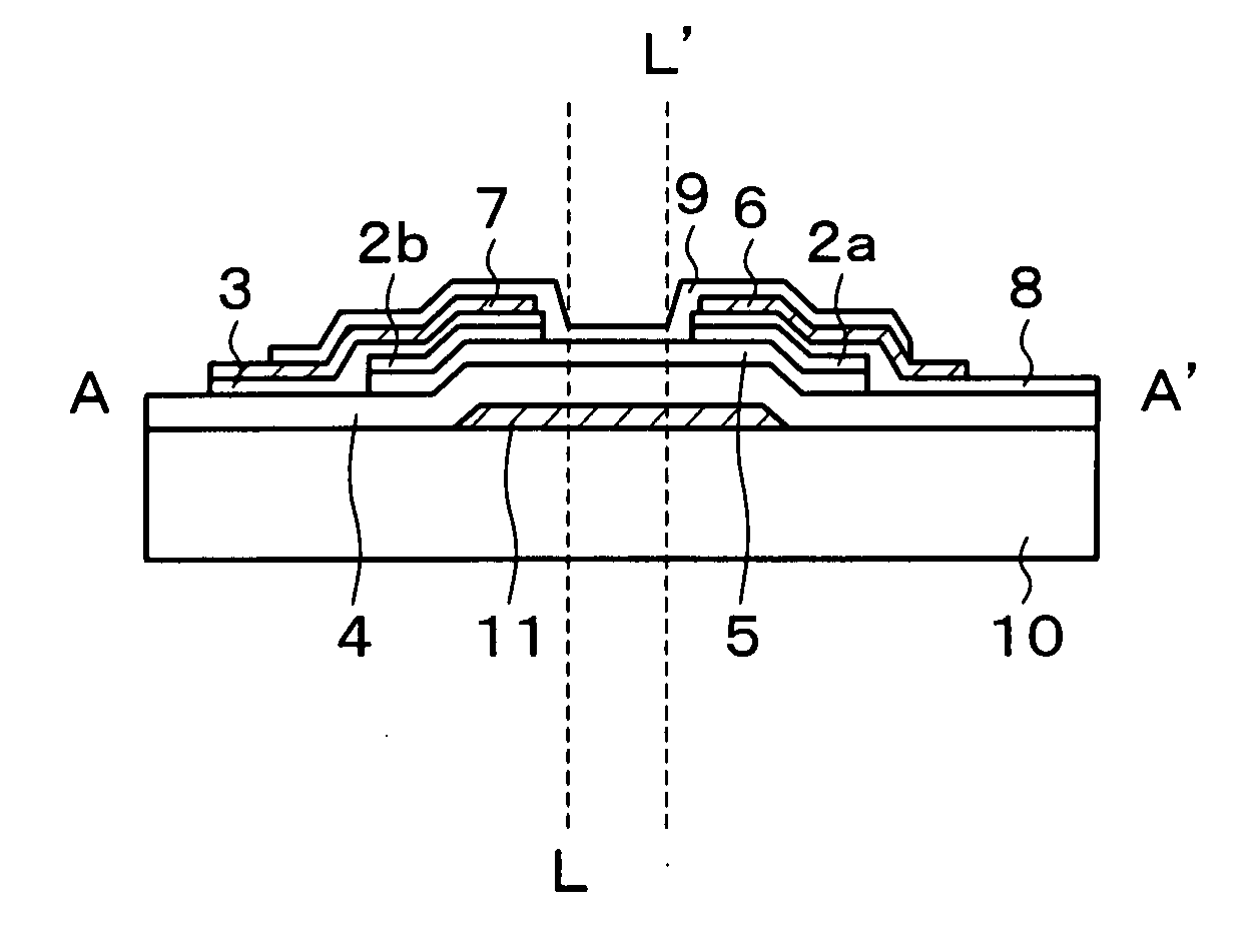
[0055] Here, FIG. 1(a) is a perspective plan view illustrating an active matrix substrate of the present invention, and FIG. 1(b) is an explanatory view showing a cross section taken along line A-A′ in FIG. 1(a).

[0056] Firstly, on a transparent insulation substrate 10 (shown in FIG. 1(b)), a metal film made of Ti, Ta, and the like is formed by the sputtering method or the like, then patterning is carried out by the photolithography so as to form a scanning line 12 and a gate electrode 11.

[0057] Next, a gate insulation film 4, a semiconductor layer, and an n-type semiconductor layer are continuously formed thereon by the plasma CVD method or the like, then a resist pattern is formed by ink jet printing. Thereafter, the semicon...


PUM


Abstract

An active matrix includes (i) a thin film transistor including a semiconductor layer formed above a gate electrode, a source electrode, and a drain electrode, the source electrode and the drain electrode formed to overlap with the semiconductor layer; and (ii) a pixel electrode connected to the drain electrode, a pixel electrode connected to the drain electrode, the drain electrode extended from the pixel electrode into a drain electrode formation region located to be kept within a semiconductor layer formation region, the drain electrode formation region sandwiched between two portions of the source electrode. With this arrangement, even when the semiconductor layers in the TFTs (thin film transistors) have unevenness in sizes, shapes, and/or formation positions thereof, it is possible to prevent occurrence of unevenness (changes) in gate-drain capacitances cgd among the TFTs. Thereby, it is possible to provide an active matrix substrate having a high display characteristic.

Description

[0001] This Nonprovisional application claims priority under 35 U.S.C. § 119(a) on Patent Application No. 2003 / 317130 file d in Japan on Sep. 9, 2003, the entire contents of which are hereby incorporated by reference. FIELD OF THE INVENTION [0002] The present invention relates to an active matrix substrate adopted (i) in a liquid crystal display device such as a liquid crystal television, a liquid crystal monitor, a laptop personal computer, and the like, or (ii) in a display device including an organic EL or the like. BACKGROUND OF THE INVENTION [0003] A liquid crystal display device is one of the most widely used flat thin display devices at present, and is applied to a laptop personal computer, a liquid crystal monitor, a liquid crystal television, and the like. A general liquid crystal display device includes two glass substrates on which transparent electrodes are provided, and between which a liquid crystal layer is sandwiched. The liquid crystal layer has transmittance which ...

Claims


Application Information

Patent Timeline
IPC IPC(8): G09F9/30G02F1/1368H01L27/01H01L27/12H01L27/32H01L29/417H01L29/423H01L29/786
CPCG02F1/1368H01L27/016H01L27/12H01L29/78696H01L29/41733H01L29/42384H01L27/3244H10K59/12
Inventor NAKAMURA, KENJIOKADA, YOSHIHIRO
Owner SHARP KK
Why Eureka
Try Eureka