Direct downlink RF module

a direct downlink and module technology, applied in the field of remote sensing, can solve the problems of difficult and expensive manufacture of structures, high-frequency antennas that are often cumbersome to manufacture, and require expensive micro-machining and hand-tuning

Inactive Publication Date: 2005-03-17
MOHAMADI FARROKH
View PDF12 Cites 42 Cited by
  • Summary
  • Abstract
  • Description
  • Claims
  • Application Information

AI Technical Summary

Benefits of technology

In accordance with another aspect of the invention, an integrated antenna array is provided that includes: a semiconductor wafer having a first surface and an opposing second surface; heavily-doped contact regions extending from the first surface to the second surface; a metallic layer on the second surface; an insulating layer on the metallic layer; a first periodic array of T-shaped dipole antenna elements formed on the insulating layer; wherein each arm of ea

Problems solved by technology

Conventional high-frequency antennas are often cumbersome to manufacture.
For example, antennas designed for 100 GHz bandwidths typically use machined waveguides as feed structures, requiring expensive micro-machining and hand-tuning.
Not only are these structures difficult and expensive to manufacture, they are also incompatible with integration to standard semiconductor processes.
As is the case with individual conventional high-frequency antennas, beam-forming arrays of such antennas are also generally difficult and expensive to manufacture.
Conventional bea

Method used


Image

  • Direct downlink RF module
  • Direct downlink RF module
  • Direct downlink RF module

Examples


Embodiment Construction

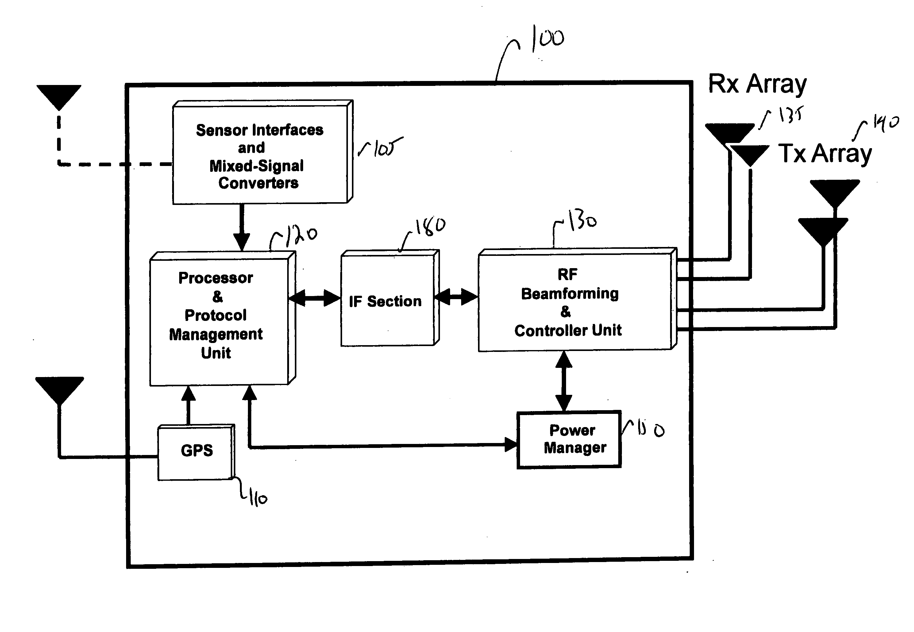
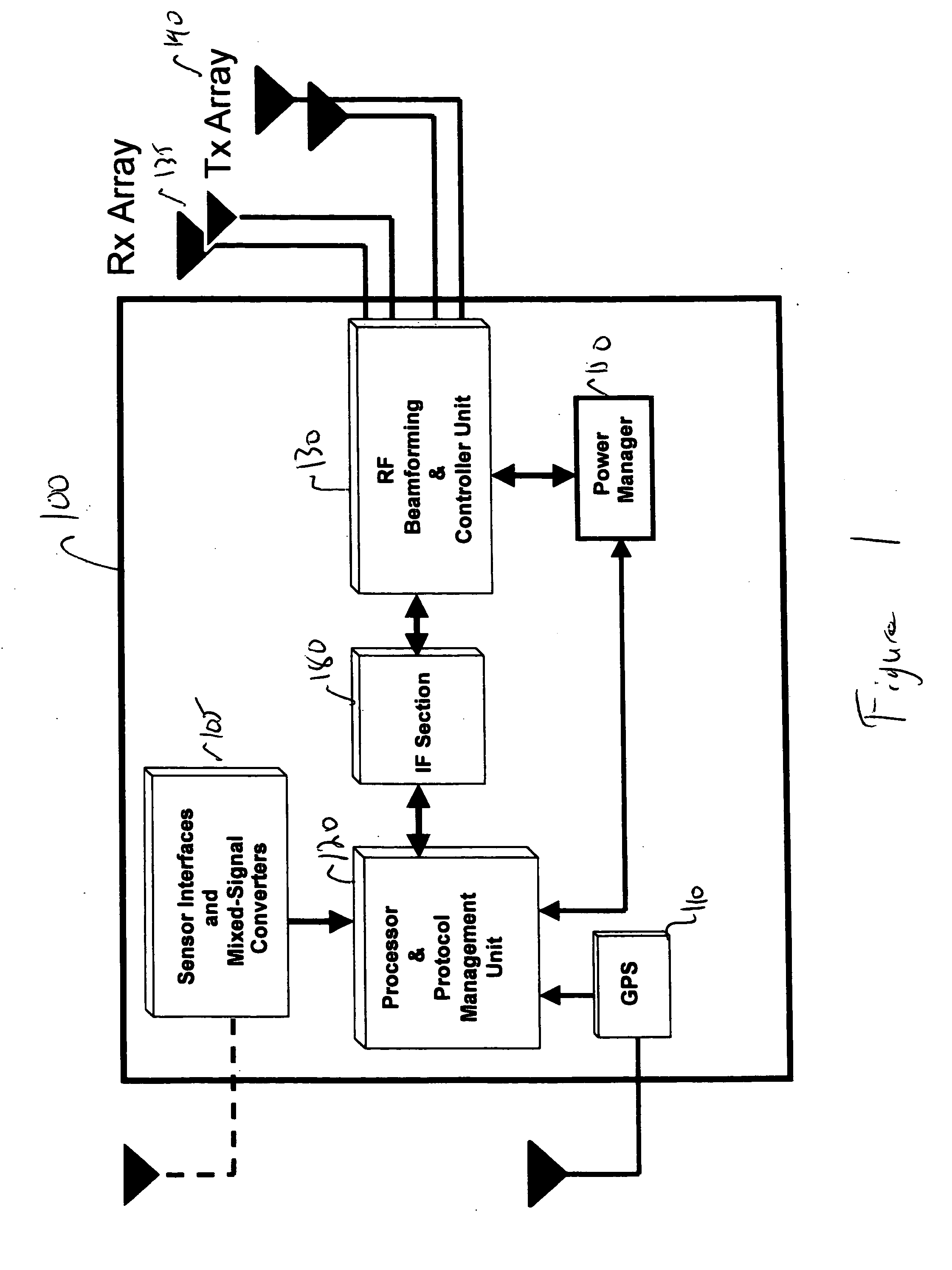
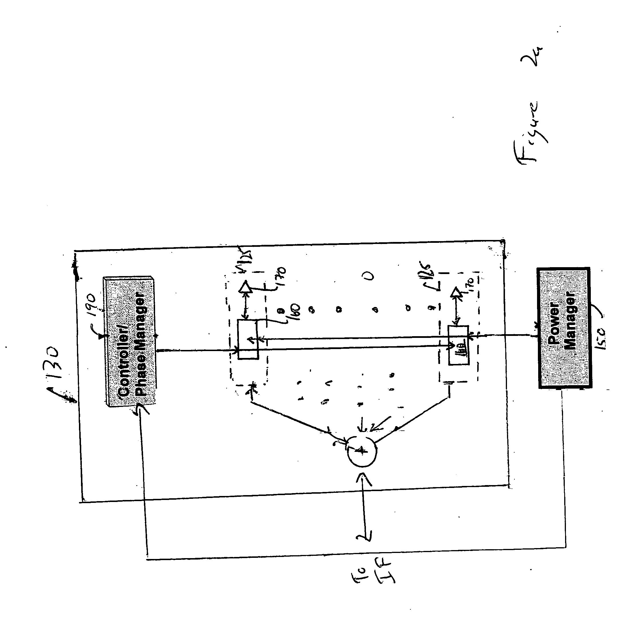
The present invention provides an RF downlink module having beam forming capabilities integrated onto a semiconductor substrate. This RF downlink module utilizes and expands upon the beam forming capabilities described in copending U.S. Ser. No. 10 / 423,303, filed Apr. 25, 2003, Ser. No. 10 / 423,106, filed Apr. 25, 2003, Ser. No. 10 / 422,907, filed Apr. 25, 2003, Ser. No. 10 / 423,129, filed Apr. 25, 2003, and Ser. No. 10 / 860,526, filed Jun. 3, 2004, the contents of all of which are hereby incorporated by reference in their entirety. A block diagram for an exemplary embodiment of an RF downlink module 100 is shown in FIG. 1. RF downlink module 100 includes sensor interfaces and analog-to-digital converters circuit 105. In general, RF downlink module 100 may be used to downlink information from any desired sensor, such as a thermal sensor, an electromagnetic sensor, an electrochemical sensor, or any other type of sensor that can sense energy or some sort and convert the sensed energy int...


PUM


Abstract

A downlink module is provided that includes a sensor interface operable to provide digital sensor signals. It also includes a GPS receiver for receiving GPS timing and location signals. The downlink module may be configured to form packets of digital sensor signals and GPS timing and location signals according to a desired protocol.

Description

TECHNICAL FIELD The present invention relates generally to remote sensing, and more particularly to an RF downlink module. BACKGROUND Conventional high-frequency antennas are often cumbersome to manufacture. For example, antennas designed for 100 GHz bandwidths typically use machined waveguides as feed structures, requiring expensive micro-machining and hand-tuning. Not only are these structures difficult and expensive to manufacture, they are also incompatible with integration to standard semiconductor processes. As is the case with individual conventional high-frequency antennas, beam-forming arrays of such antennas are also generally difficult and expensive to manufacture. Conventional beam-forming arrays require complicated feed structures and phase-shifters that are impractical to be implemented in a semiconductor-based design due to its cost, power consumption and deficiency in electrical characteristics such as insertion loss and quantization noise levels. In addition, con...

Claims


Application Information

Patent Timeline
IPC IPC(8): H01Q3/26H01Q11/10H01Q21/00
CPCH01Q3/26H01Q21/0087H01Q21/0025H01Q11/105H04B7/15528
Inventor MOHAMADI, FARROKH
Owner MOHAMADI FARROKH
Why Eureka
Try Eureka