


Quick Research
Generate reliable direction feasibility study reports for your R&D in just a few steps.

Technical Q&A
Discover and master advanced knowledge NOW. Basics, ideas, possibilities, all at once.

Find Solutions
As an expert in R&D theories, this can generate solutions to your technical problems instantly.

Evaluate Feasibility
Analyze your overall solution with one click, know your potential R&D risks in advance.

Monitor Landscape
Get weekly tech updates, stay abreast of the latest tech innovations and key insights.
Combined semiconductor device, LED print head, and image forming apparatus
a semiconductor device and print head technology, applied in the direction of semiconductor devices, printing, electrical equipment, etc., can solve the problems of difficult to solve, difficult to achieve significant reductions in material cost, poor material usage efficiency, etc., to save semiconductor materials, eliminate wire-bonding pads, and reduce associated material costs
- Summary
- Abstract
- Description
- Claims
- Application Information
AI Technical Summary
Benefits of technology
Problems solved by technology
Method used
Image

Examples
first embodiment
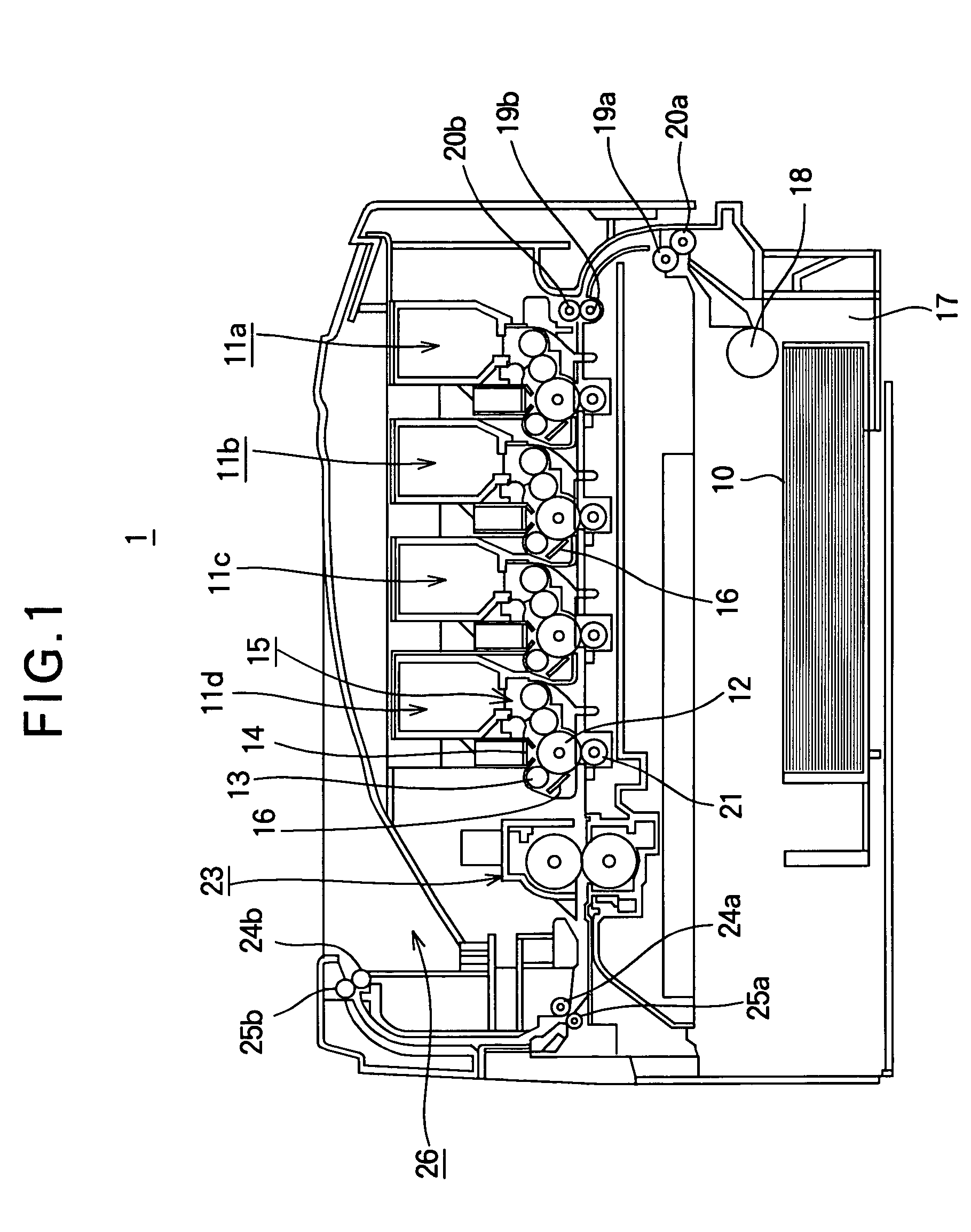
Referring to FIG. 1, a first embodiment of the invention is an electrophotographic apparatus 1 for forming color images on printing media 10. The image forming apparatus 1 comprises four process units 11a-11d that form yellow, magenta, cyan, and black images, respectively. Each process unit includes a photosensitive drum 12 on which the image of the corresponding color is formed. Disposed around the photosensitive drum 12 are a charging unit 13 that supplies current to the photosensitive drum 12 to charge the surface thereof, an LED print head 14 that selectively illuminates the charged surface of the photosensitive drum 12 to form an electrostatic latent image, a developing unit 15 that supplies toner particles of the appropriate color to the surface of the photosensitive drum 12 to develop the electrostatic latent image, and a cleaning unit 16 that removes remaining toner from the photosensitive drum 12 after the developed image has been transferred to the printing media 10.
The...
second embodiment
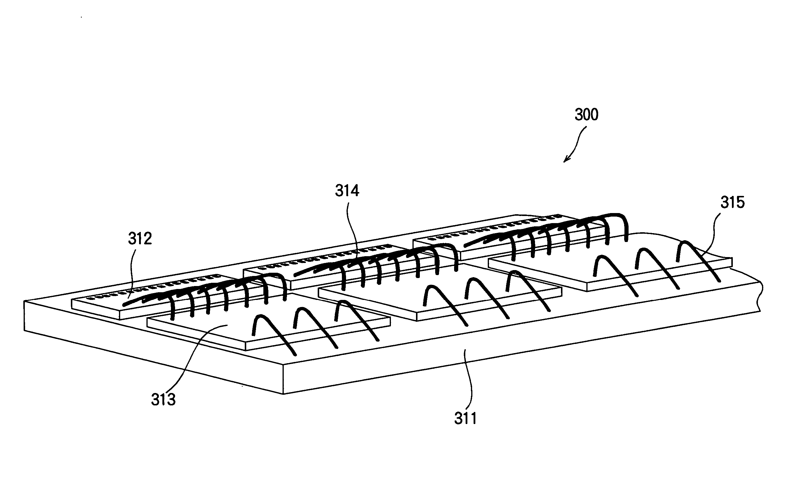
In the first embodiment described above, a smaller semiconductor device is obtained by attaching thin-film light-emitting elements and thin-film driver elements to a transparent substrate and interconnecting them by means of electrodes, thereby eliminating the necessity of providing large wire bonding pads and bonding wires for both elements. Since the light-emitting elements are attached to the transparent substrate after the driver elements have already been formed, however, if the attachment of any one of the light-emitting elements fails, the entire device, including the transparent substrate and the driver elements, becomes defective. A possible consequence is reduced fabrication yields. In the second embodiment, described below, the light-emitting elements are attached to a supporting substrate separate from the transparent substrate and then the two substrates are bonded together, thereby limiting the impact of the quality of the attachment of the light-emitting elements on ...
third embodiment
In the second embodiment described above, since the light-emitting elements are disposed on the supporting substrate and the driving circuitry is disposed on the transparent substrate, electrode pads are necessary to interconnect the light-emitting elements with the driving circuitry. Although these electrode pads are smaller than conventional wire bonding pads, it would be desirable to eliminate them completely, to reduce the size of the transparent substrate. In the third embodiment described below, this is done by placing both the light-emitting elements and the driver elements on the supporting substrate.
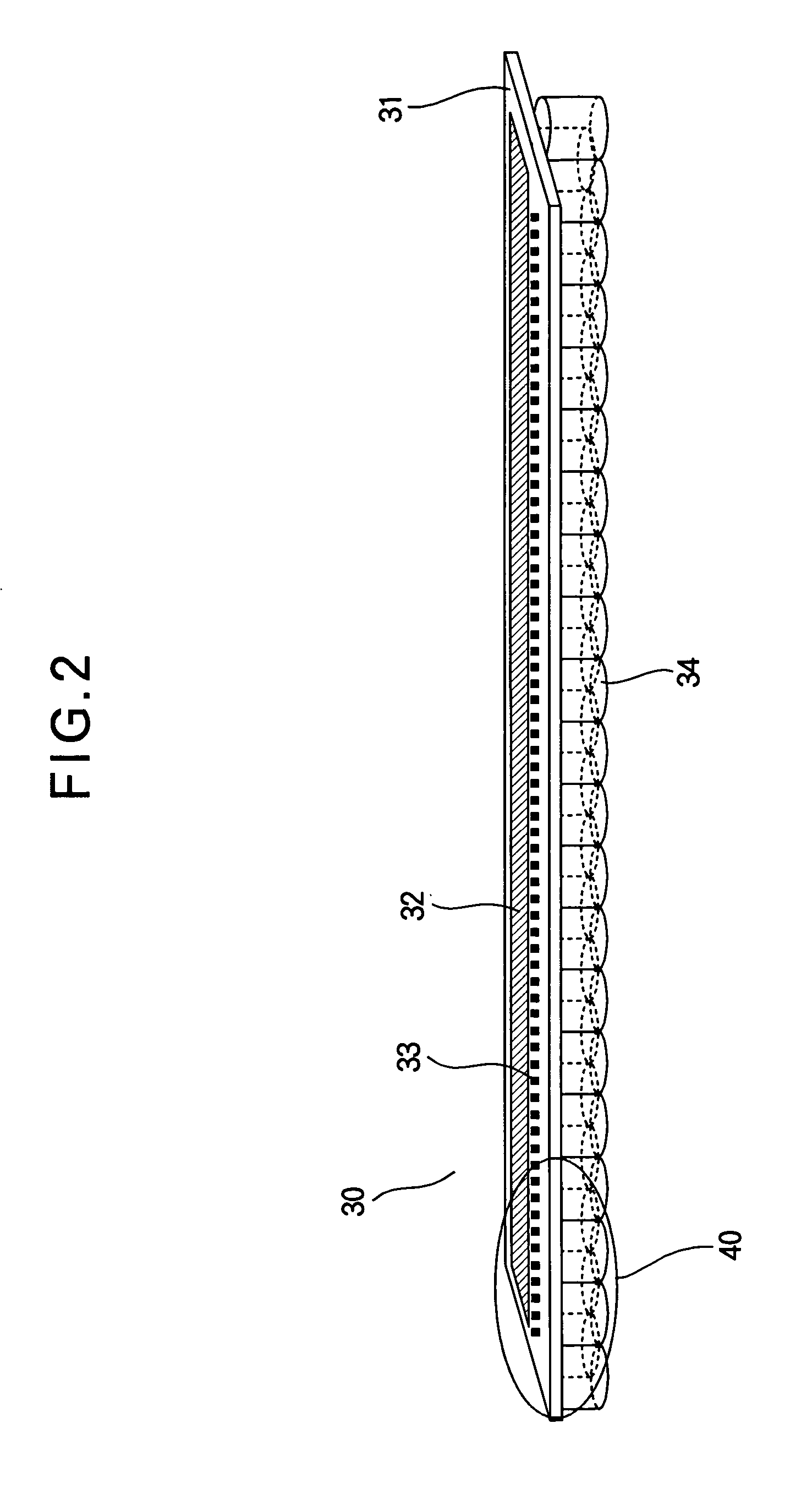
FIG. 20A is a plan view illustrating the upper surface of an exemplary supporting substrate 111 on which the light-emitting elements and driver elements are disposed, and FIG. 20B is a section through line C-C in FIG. 20A. The supporting substrate 111 in FIGS. 20A and 20B is, for example, a silicon substrate, the surface of which is covered by a metal layer 118. The metal laye...
PUM
 Abstract
Description
Claims
Application Information
 - R&D Engineer
- R&D Manager
- IP Professional
- Industry Leading Data Capabilities
- Powerful AI technology
- Patent DNA Extraction
Browse by: Latest US Patents, China's latest patents, Technical Efficacy Thesaurus, Application Domain, Technology Topic, Popular Technical Reports.
© 2024 PatSnap. All rights reserved.Legal|Privacy policy|Modern Slavery Act Transparency Statement|Sitemap|About US| Contact US: help@patsnap.com