Manufacturing method for microdisplay

Inactive Publication Date: 2005-03-17
CHEN SHENG LUNG +1
View PDF12 Cites 21 Cited by
  • Summary
  • Abstract
  • Description
  • Claims
  • Application Information

AI Technical Summary

Benefits of technology

[0011] The present invention provides a manufacturing method of a microdisplay f

Problems solved by technology

Such uniformity of gaps between the wafer substrate and the

Method used


Image

  • Manufacturing method for microdisplay
  • Manufacturing method for microdisplay
  • Manufacturing method for microdisplay

Examples


Example

[0025] First Embodiment

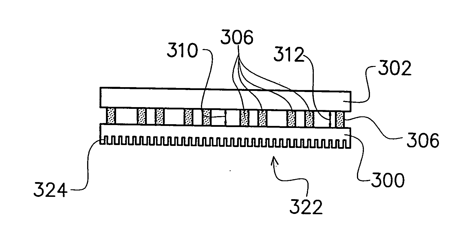
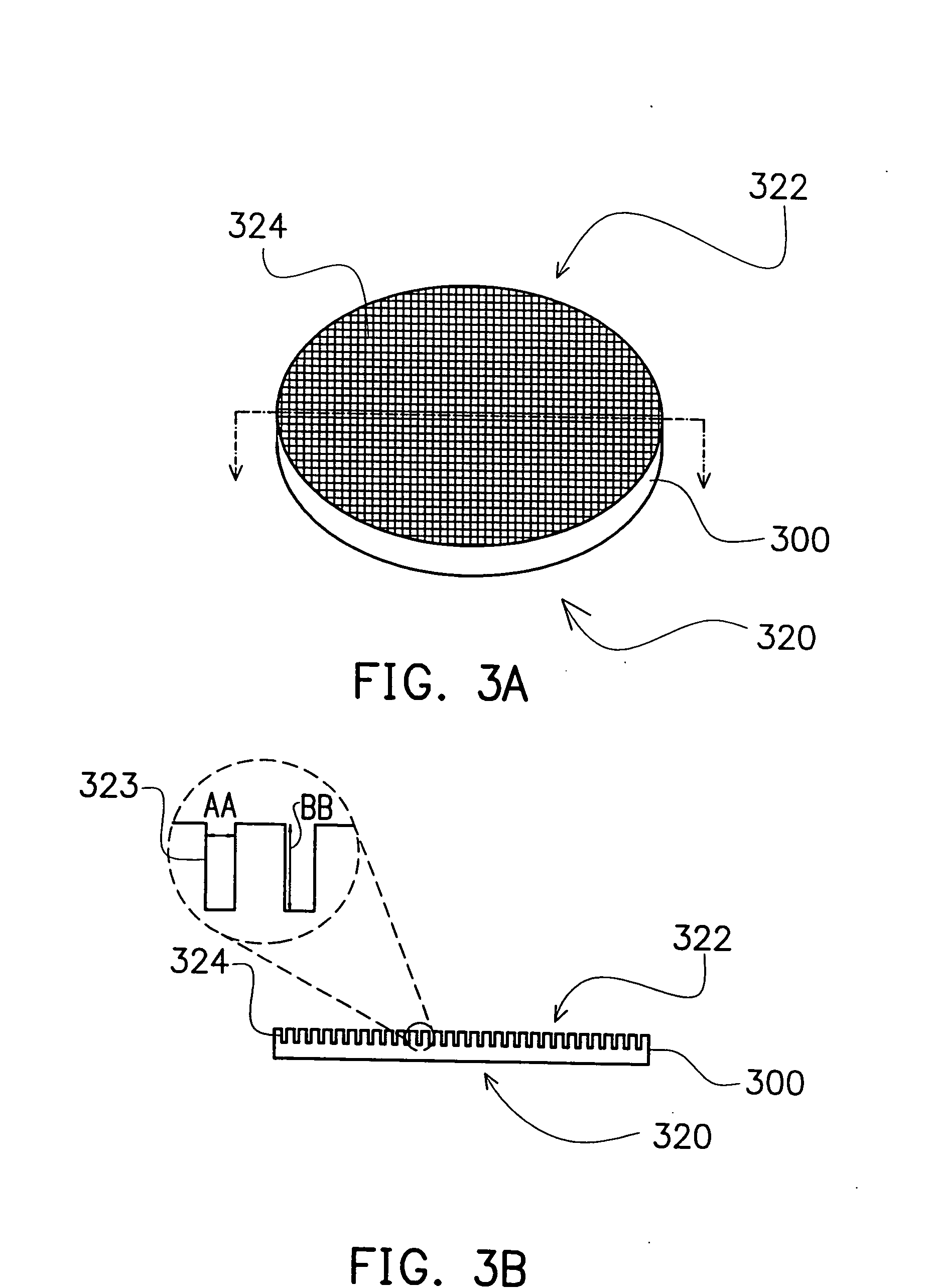
[0026]FIG. 3A is a three-dimensional view of a wafer substrate for a microdisplay after cutting according to the first preferred embodiment of the present invention, while FIG. 3B is a cross-sectional view of the wafer substrate of FIG. 3A. Referring to FIGS. 3A and 3B, a wafer substrate 300 is provided, while a plurality of pixel structures 304 (shown in FIG. 4) are formed on the front side 320 of the wafer substrate 300. For example, the wafer substrate 300 is a silicon wafer substrate. The backside 322 of the wafer substrate 300 is cut or sectioned in order to form trenches 323 with a pattern 324. The trenches are formed in a grid pattern or a checker pattern, or in other arranged patterns. As shown in an enlarged view (left side) for a portion of the wafer substrate in FIG. 3B, the trenches 323 of the grid pattern 324 have a width AA of about 50-150 microns and a depth BB of about 50-300 microns. For example, laser cutting is used to perform the cutting o...

Example

[0031] Second Embodiment

[0032]FIG. 7 is a flow chart showing the process steps for improving uniformity of the microdisplay according to the second preferred embodiment of the present invention. In step 700, a first substrate is provided with a plurality of pixel structures formed on the front side of the first substrate. In step 702, the backside of the first substrate is sectioned (cut) to form trenches with a pattern. The trenches are formed in a grid pattern or a checker pattern, or in other arranged patterns by, for example, laser cutting, while the trenches have a width of about 50-150 microns and a depth of about 50-300 microns.

[0033] In step 704, a sealant pattern is formed on the front side of the first substrate. In step 706, a second substrate is arranged above the front side of the first substrate, so that the first substrate is adhered to the second substrate.

[0034] In conclusion, the present invention has the following advantages:

[0035] Since the backside of the wa...


PUM


Abstract

The present invention provides a manufacturing method for a microdisplay. After providing a wafer with a plurality of pixel structures on the front side, trenches with a pattern are formed on the backside of the wafer. A transparent plate is disposed above the front side of the wafer and a sealant is applied to join the wafer and the transparent plate. After cutting the wafer and the transparent plate into display cells of suitable sizes, liquid crystal is then introduced in-between the sealant of the display cells.

Description

CROSS-REFERENCE TO RELATED APPLICATION [0001] This application claims the priority benefit of Taiwan application serial no. 92106446, filed Mar. 24, 2003. BACKGROUND OF THE INVENTION [0002] 1. Field of Invention [0003] The present invention relates to a manufacturing method of a microdisplay. More particularly, the present invention relates to a manufacturing method for improving the non-uniformity of the microdisplay. [0004] 2. Description of Related Art [0005] Liquid crystal pixel structure has been widely applied in daily life applications, including liquid crystal televisions, liquid crystal monitors of portable computers or desktop personal computers and liquid crystal projectors. For large-scale displays, the liquid crystal projectors are particularly important. The core element of the liquid crystal projector is the optical engine that generally includes a light source, an optical component consisting of prism pairs and several liquid crystal panels (LCPs) corresponding to di...

Claims


Application Information

Patent Timeline
IPC IPC(8): G02F1/1341G02F1/1362
CPCG02F1/136277G02F1/1341
Inventor CHEN, SHENG-LUNGKUAN, DA-SHUANG
Owner CHEN SHENG LUNG
Why Eureka
Try Eureka