Field effect devices having a gate controlled via a nanotube switching element

a technology of nanotube switching element and field effect, which is applied in the direction of discharge tube luminescnet screen, pulse technique, instruments, etc., can solve the problems of low relative speed, power consumption, and long write cycle (ms) in comparison to dram or sram, and achieves relatively low cost but cannot be rewritten

Active Publication Date: 2005-03-24
NANTERO
View PDF10 Cites 81 Cited by
  • Summary
  • Abstract
  • Description
  • Claims
  • Application Information

AI Technical Summary

Problems solved by technology

ROM is relatively low cost but cannot be rewritten.
EEPROM (or “Flash”) is inexpensive, and has low power consumption but has long write cycles (ms) and low relative speed in comparison to DRAM or SRAM.
Flash also has a finite number of read / write cycles leading to low long-term reliability.
SRAM does not need to be refreshed and is fast relative to DRAM, but has lower density and is more expensive relative to DRAM.
Both SRAM and DRAM are volatile, meaning that if power to the memory is interrupted the memory will lose the information stored in the memory cells.
Consequently, existing technologies are either non-volatile but are not randomly accessible and have low density, high cost, and limited ability to allow multiple writes with high reliability of the circuit's function, or they are volatile and complicate system design or have low density.
A different memory cell based upon magnetic tunnel junctions has also been examined but has not led to large-scale commercialized MRAM devices.
FRAM suffers from a large memory cell size, and it is difficult to manufacture as a large-scale integrated component.
While the nonvolatility condition is met, this technology appears to suffer from slow operations, difficulty of manufacture and poor reliability and has not reached a state of commercialization.
This form of memory requires highly specialized wire junctions and may not retain non-volatilely owing to the inherent instability found in redox processes.

Method used


Image

  • Field effect devices having a gate controlled via a nanotube switching element
  • Field effect devices having a gate controlled via a nanotube switching element
  • Field effect devices having a gate controlled via a nanotube switching element

Examples


Embodiment Construction

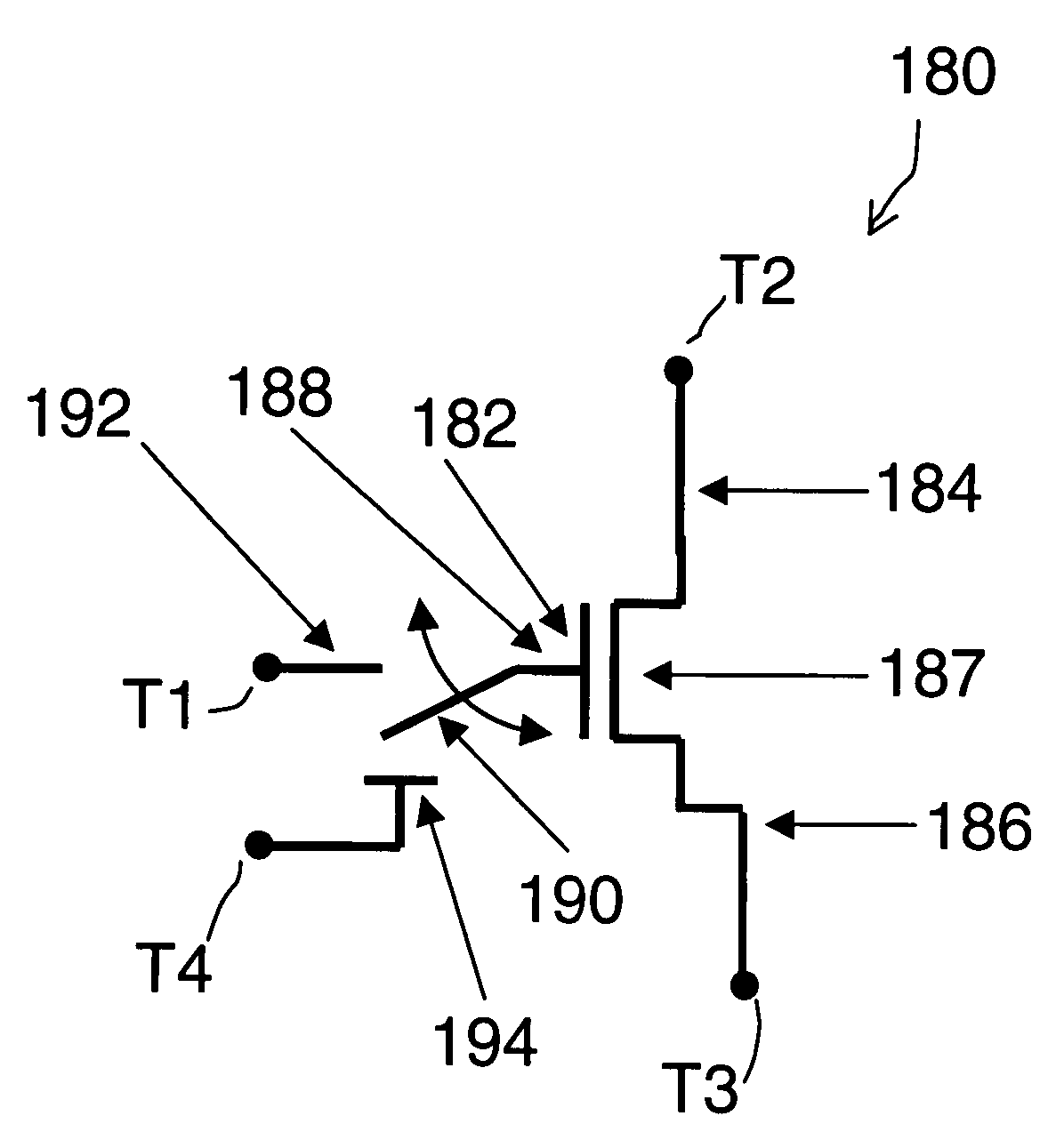
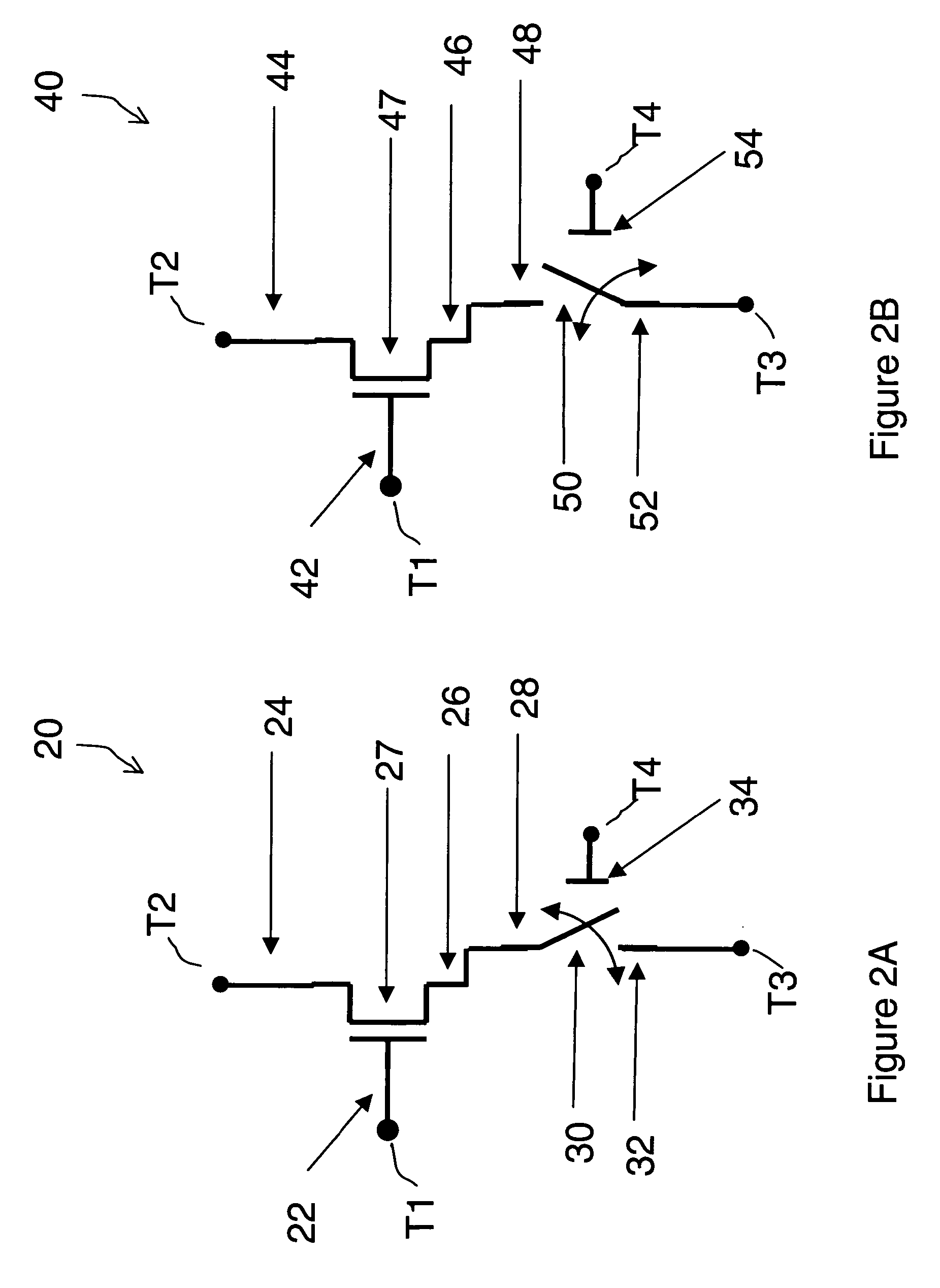
[0103] Preferred embodiments of the invention provide a field effect device that acts like a FET in its ability to create an electronic communication channel between a drain and a source node, under the control of a gate node. However, the preferred field effect devices further include a separate control structure to non-volatilely control the electrical capabilities of the field effect device. More specifically, the control structure uses carbon nanotubes to provide non-volatile switching capability that independently control the operation of the drain, source, or gate node of the field effect device. By doing so, the control structure provides non-volatile state behavior to the field effect device. Certain embodiments provide non-volatile RAM structures. Preferred embodiments are scalable to large memory array structures. Preferred embodiments use processes that are compatible with CMOS circuit manufacture. While the illustrations combine NMOS FETs with carbon nanotubes, it should...


PUM


Abstract

Field effect devices having a gate controlled via a nanotube switching element. Under one embodiment, a non-volatile transistor device includes a source region and a drain region of a first semiconductor type of material and each in electrical communication with a respective terminal. A channel region of a second semiconductor type of material is disposed between the source and drain region. A gate structure is disposed over an insulator over the channel region and has a corresponding terminal. A nanotube switching element is responsive to a first control terminal and a second control terminal and is electrically positioned in series between the gate structure and the terminal corresponding to the gate structure. The nanotube switching element is electromechanically operable to one of an open and closed state to thereby open or close an electrical communication path between the gate structure and its corresponding terminal. When the nanotube switching element is in the closed state, the channel conductivity and operation of the device is responsive to electrical stimulus at the terminals corresponding to the source and drain regions and the gate structure.

Description

CROSS REFERENCE TO RELATED APPLICATIONS [0001] This application claims priority under 35 U.S.C. § 19(e) to U.S. Provisional Patent Application No. 60 / 476,976, filed on Jun. 9, 2003, entitled Non-Volatile Electromechanical Field Effect Transistors and Methods of Forming Same, which is incorporated herein by reference in its entirety. [0002] This application is related to the following U.S. applications, the contents of which are incorporated herein in their entirety by reference: [0003] U.S. patent apl. Ser. No. 10 / 810,962, filed Mar. 26, 2004, entitled NRAM BIT SELECTABLE TWO-DEVICE NANOTUBE ARRAY; [0004] U.S. patent apl. Ser. No. 10 / 810,963, filed Mar. 26, 2004, entitled NRAM BYTE / BLOCK RELEASED BIT SELECTABLE ONE-DEVICE NANOTUBE ARRAY; [0005] U.S. patent apl. Ser. No. 10 / 811,191, filed Mar. 26, 2004, entitled SINGLE TRANSISTOR WITH INTEGRATED NANOTUBE (NT-FET); and [0006] U.S. patent apl. Ser. No. 10 / 811,356, filed Mar. 26, 2004, entitled NANOTUBE-ON-GATE FET STRUCTURES AND APPLIC...

Claims


Application Information

Patent Timeline
Patent Type & Authority Applications(United States)
IPC IPC(8): G11C7/06G11C8/02G11C11/00G11C11/50G11C13/02G11C16/02G11C16/04G11C17/16G11C23/00H01H59/00H01J1/62H01LH01L21/336H01L21/82H01L21/8246H01L27/112H01L27/115H01L27/28H01L29/06H01L29/423H01L29/739H01L29/745H01L29/76H01L51/00H01L51/05H01L51/30H03K17/16
CPCB82Y10/00H01L27/1052G11C13/025G11C16/0416G11C17/16G11C17/165G11C23/00G11C2213/16G11C2213/17G11C2213/79H01H1/0094H01L27/10H01L27/112H01L27/11206H01L27/115H01L27/286H01L29/0665H01L29/0673H01L29/42324H01L51/0048H01L51/0052H01L51/0508B82Y99/00H01L29/78Y10S977/742Y10S977/762Y10S977/936Y10S977/943Y10S977/938Y10S977/724Y10S977/708Y10S977/94G11C7/065H10B99/00H10B20/20H10B20/00H10B69/00H10K19/20H10K85/221H10K85/615H10K10/46
Inventor BERTIN, CLAUDE L.RUECKES, THOMASSEGAL, BRENT M.
Owner NANTERO
Why Eureka
Try Eureka