

Method of fabricating SiC semiconductor device
a technology of semiconductor devices and semiconductors, applied in the direction of semiconductor devices, basic electric elements, electrical equipment, etc., can solve the problems of difficult nullification of remaining carbon and high interface level density, and achieve the effects of low interface level density, good channel mobility, and reduced carbon remaining
- Summary
- Abstract
- Description
- Claims
- Application Information
AI Technical Summary
Benefits of technology
Problems solved by technology
Method used
Image

Examples
first embodiment
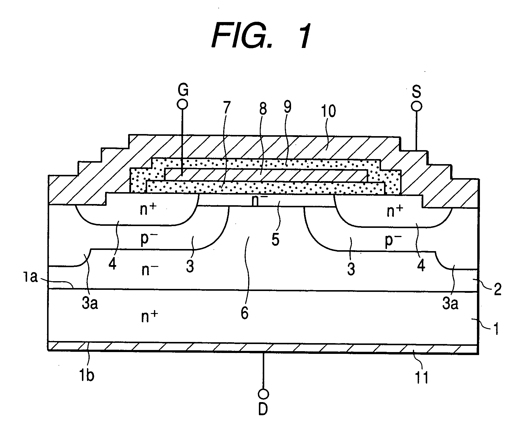
[0065]FIG. 1 shows an n-channel planar MOSFET fabricated according to a first embodiment of this invention. The n-channel planar MOSFET is also referred to as an n-channel vertical power MOSFET.
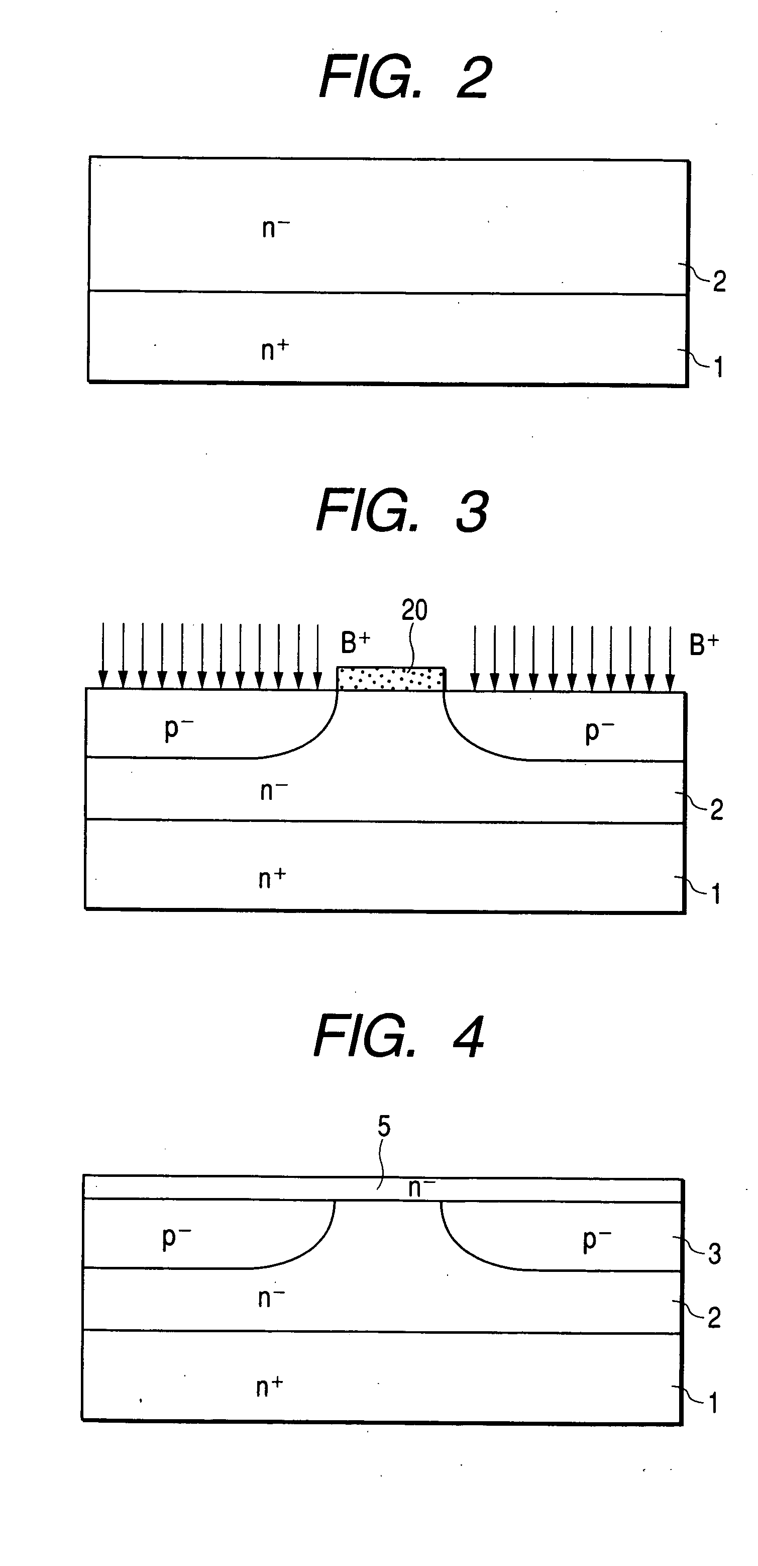
[0066] The vertical power MOSFET in FIG. 1 includes an n+ type substrate 1 made of silicon carbide (SiC). The n+ type substrate 1 has an upper surface constituting a main surface 1a, and a lower surface constituting a back surface 1b opposite to the main surface 1a. An n− type drift layer 2 made of SiC is superposed on the main surface 1a of the n+ type substrate 1. The n− type drift layer 2 is lower in dopant concentration than the n+ type substrate 1. Thus, the n− type drift layer 2 is higher in resistivity than the n+ type substrate 1. The main surface 1a of the n+ type substrate 1 and an upper surface of the n− type drift layer 2 agree with (0001) planes. Thus, regarding crystals forming the n+ type substrate 1 and the n− type drift layer 2, orientation (plane orientation) causing a lowe...
second embodiment
[0094] A second embodiment of this invention is similar to the first embodiment thereof except for design changes mentioned hereafter.
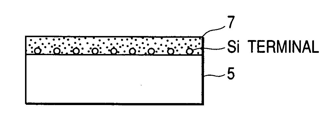
[0095] According to the second embodiment of this invention, after the exposed surface of the surface channel layer 5 is processed into a Si-terminated cleaned surface, a protective film is deposited on the surface of the surface channel layer 5 in an ultra-high vacuum chamber. The protective film includes an SiOx film or a nitride film. The protective film prevents impurity from adhering to the surface of the surface channel layer 5. Thus, a high interface level density caused by impurity is prevented from occurring.
[0096] In the case where the protective film includes a nitride film, an ONO film composed of the protective film and an SiO2 film provided on the surface of the surface channel layer 5 can be used instead of the gate oxide film 7.
third embodiment
[0097] A third embodiment of this invention is similar to the first embodiment thereof except for design changes mentioned hereafter.
[0098] The third embodiment of this invention is designed to reduce the amount of carbon remaining in the interface between the gate oxide film 7 and the surface channel layer 5 according to a modified procedure.
[0099] After the removal of the LTO film 22 (see FIGS. 6 and 7), the exposed surfaces of the semiconductor body are cleaned. Thereafter, as shown in FIG. 19, a Si layer 30 is formed on an upper surface of the surface channel layer 5. As in the first embodiment of this invention, the Si layer 30 is processed so that the upper surface of the surface channel layer 5 becomes an Si-terminated cleaned surface of a 3×3 structure, a 2·31 / 2×2·131 / 2 structure, a 31 / 2×31 / 2 structure, or a 6×6 structure (see FIG. 20).
[0100] Subsequently, as shown in FIG. 21, a gate oxide film 7 is deposited on the upper surface of the surface channel layer 5. The gate o...
PUM
| Property | Measurement | Unit |
|---|---|---|
| temperature | aaaaa | aaaaa |
| temperature | aaaaa | aaaaa |
| temperature | aaaaa | aaaaa |
Abstract
Description
Claims
Application Information