

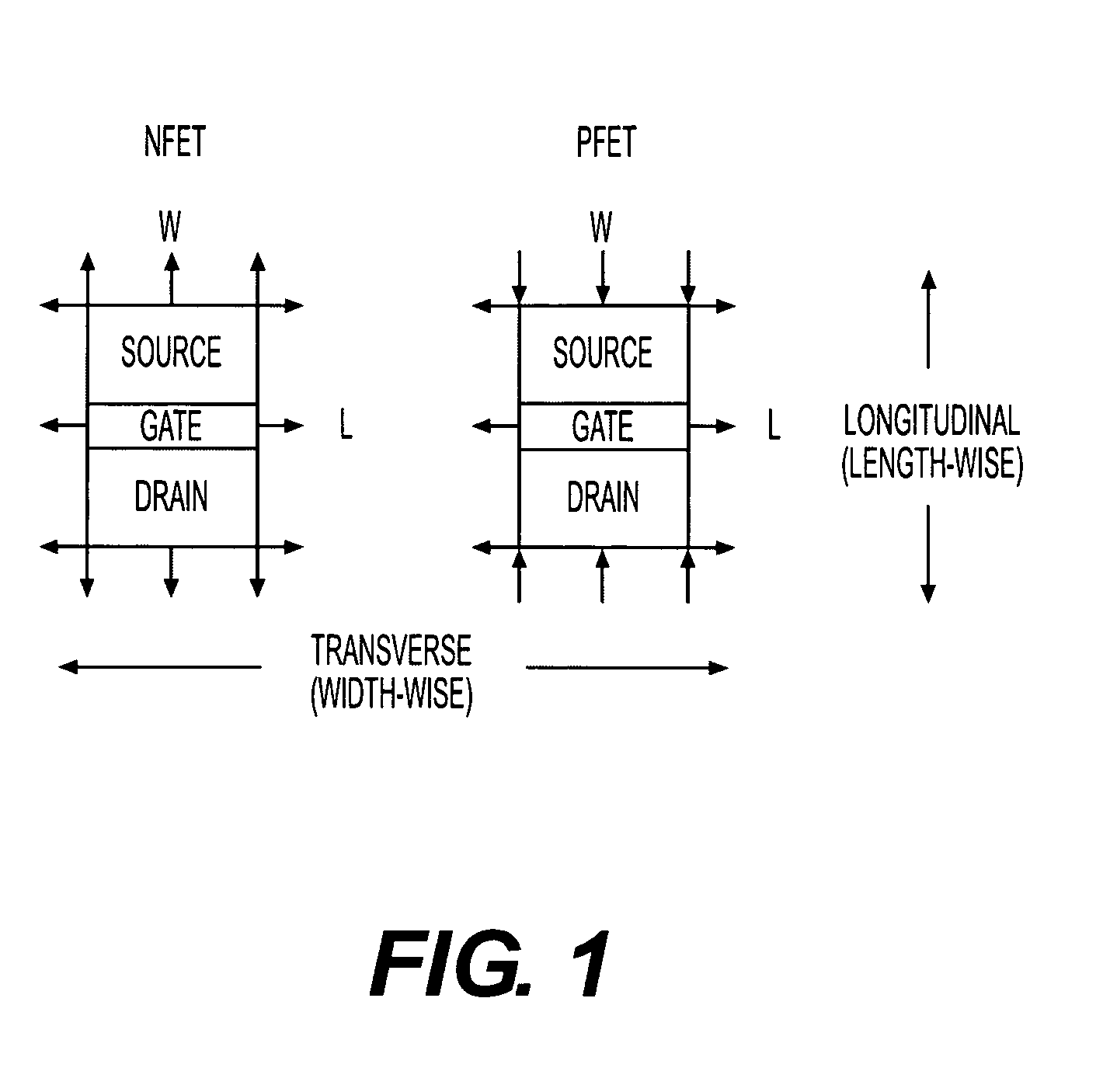
NFETs using gate induced stress modulation
a technology of gate induced stress and gate induced stress, which is applied in the direction of semiconductor devices, electrical equipment, basic electric elements, etc., can solve the problems of higher cost, disadvantageous to the performance of the pfet, and beneficial to the performance of the n
- Summary
- Abstract
- Description
- Claims
- Application Information
AI Technical Summary
Benefits of technology
Problems solved by technology
Method used
Image

Examples
Embodiment Construction
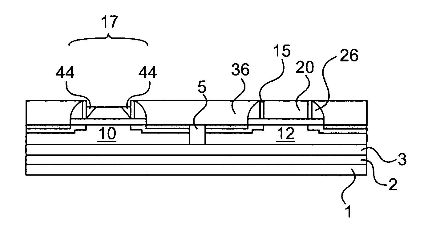
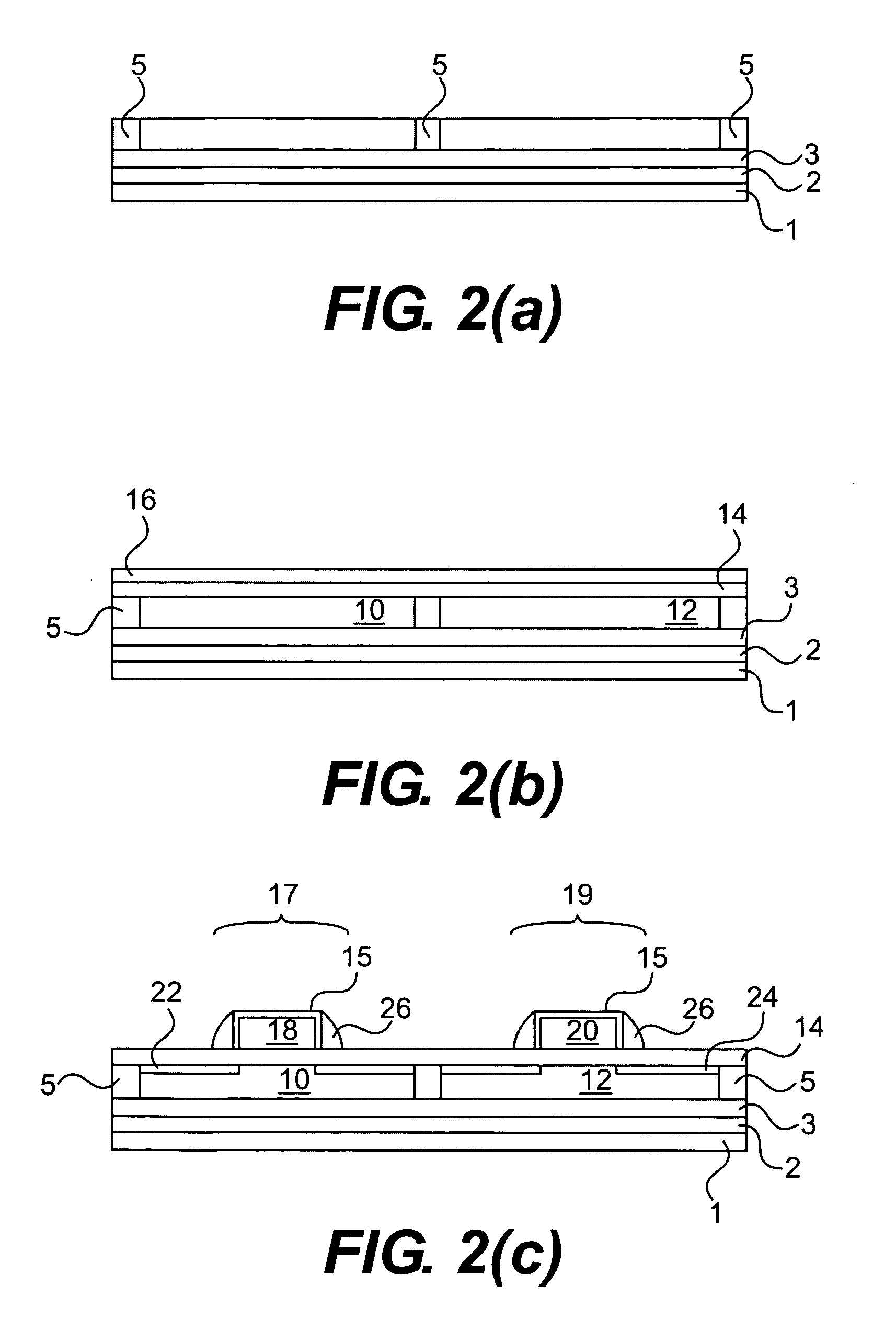
[0017] The invention provides a method for fabricating devices with improved performance characteristics. In this invention, oxidation of the gate polysilicon is used to control the stresses in complimentary metal oxide semiconductor (CMOS) NFET devices such that their performances are enhanced without degrading the performance of the PFET devices.
[0018] In one aspect of the invention, polysilicon of an NFET gate is oxidized while the polysilicon of a PFET gate is masked to prevent the polysilicon of the PFET from being oxidized. By preventing the oxidation of the polysilicon of the PFET, degradation of hole mobility is prevented. In this aspect, the oxidation of NFET gates creates tensile stresses in the channels of the NFETs without creating tensile stresses in the channel of the PFETs. By oxidizing the gate polysilicon of the NFETs large stresses of about 500 MPa to about 1000 MPa, for example, are formed in a channel of the NFET. In one implementation the stresses are about 700...
PUM
 Abstract
Description
Claims
Application Information