
High capacitive density stacked decoupling capacitor structure

Active Publication Date: 2005-03-24
TEXAS INSTR INC
View PDF2 Cites 4 Cited by
  • Summary
  • Abstract
  • Description
  • Claims
  • Application Information

AI Technical Summary

Problems solved by technology

For example, the advancement affects numerous device attributes and increases the need for attention to such attributes during design and manufacturing, where such attributes include device size, reliability, yield, and cost.
While polysilicon to N-well decoupling capacitors have been used successfully in various devices, various drawbacks have been observed in such devices as performance demands increase.
Thus, when using polysilicon to N-well decoupling capacitors in an attempt to satisfy demands, there is a trade-off in that larger amounts of chip area are required to implement the capacitors, where it is well-known that such area can be quite costly in terms of design and, indeed, in some instances, prohibitive.
However, there also is a trend in the transistor art to decease the thickness of these gate dielectrics, which correspondingly decreases the amount of capacitive material in the polysilicon to N-well decoupling capacitors.
Such a result is undesirable for the capacitor for two reasons.
First, it increases the chance of capacitor leakage because the likelihood of leakage increases as dielectric thickness decreases and the need for decoupling increases.
Second, with a thinner capacitive dielectric, there is a greater chance of an electrical short-circuit through the dielectric and, hence, between the capacitor plates.
The N-well in such a case may provide some resistance to the current flowing through the short-circuit so as to prevent a total device failure, yet the decoupling effect is lost and, hence, with a sufficient number of such failures then device yield is reduced and / or circuit performance is reduced.

Method used


Image

  • High capacitive density stacked decoupling capacitor structure
  • High capacitive density stacked decoupling capacitor structure
  • High capacitive density stacked decoupling capacitor structure

Examples


Embodiment Construction

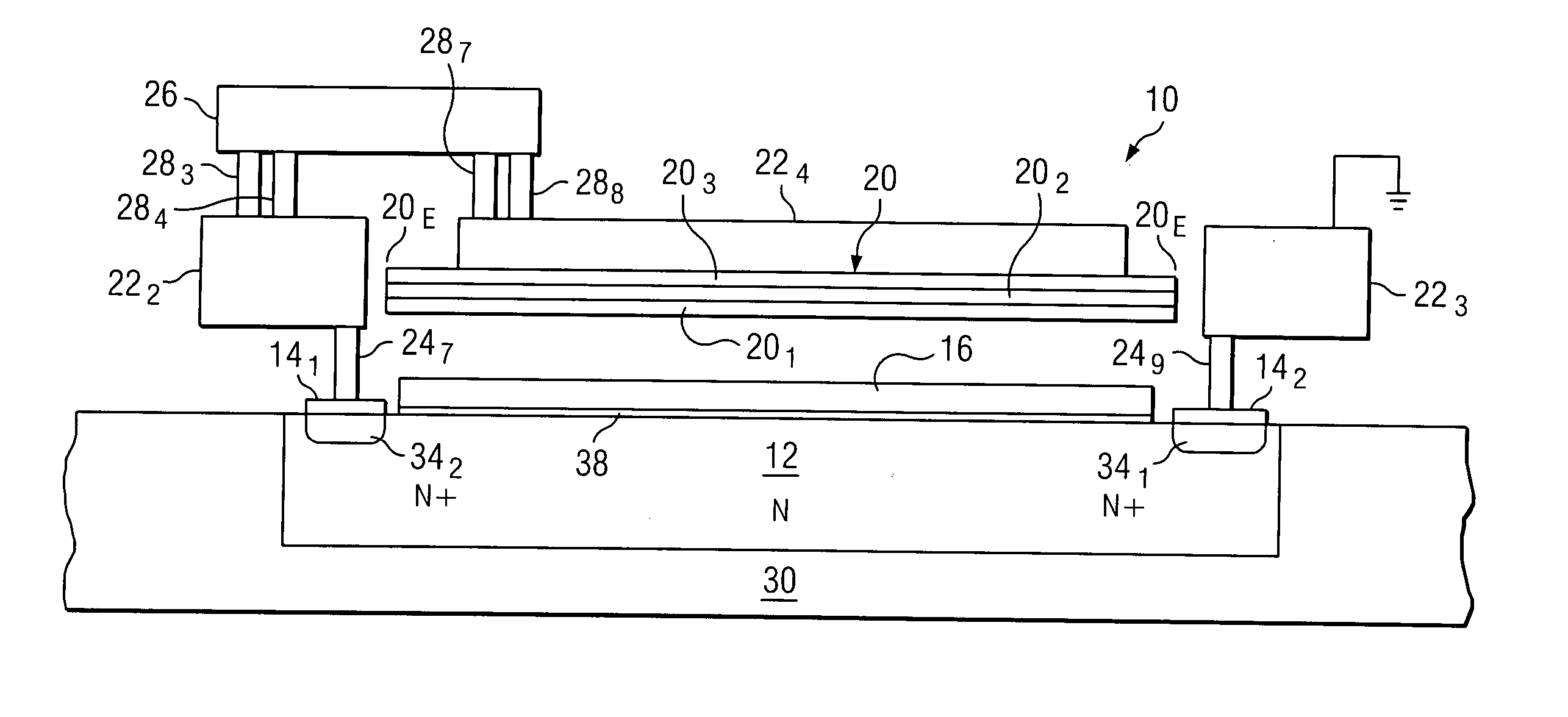
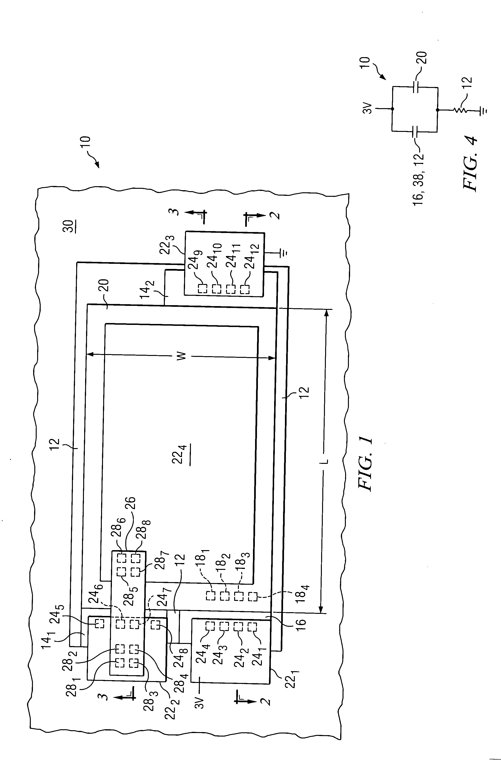
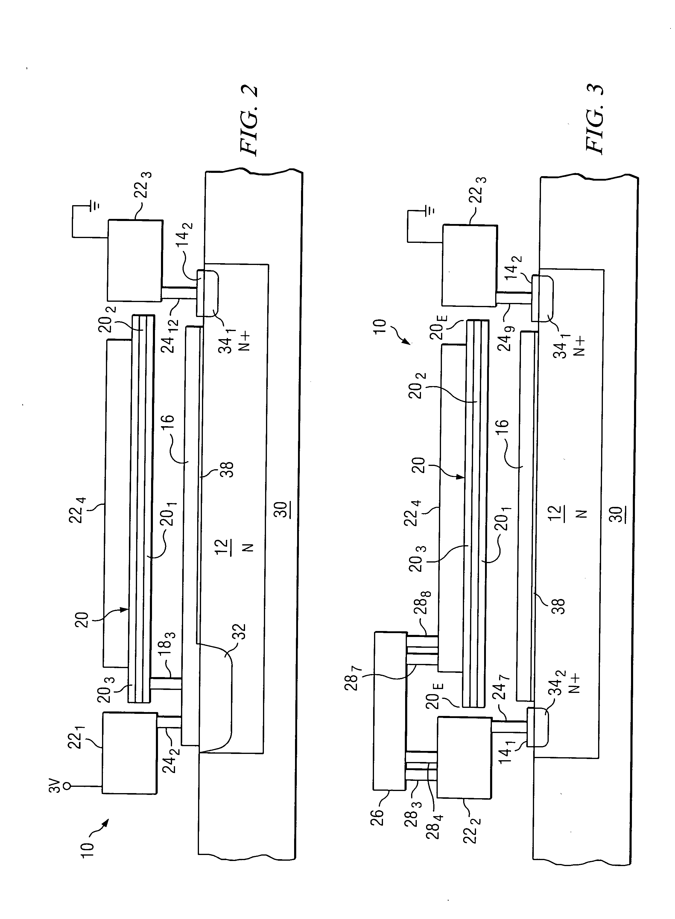
[0014]FIG. 1 illustrates a top view of a decouplng capacitor structure 10 according to the preferred embodiment and built within a semiconductor integrated circuit. Structure 10, as explored further below in connection with FIGS. 2 and 3, is constructed using numerous layers from which various components are formed. Proceeding generally from a bottom-to-top approach in FIG. 1, structure 10 includes a well 12, preferably of an N-type material. Toward the top left and bottom right of structure 10 are two silicide regions 141 and 142 where active doped regions are underneath regions 141 and 142 but those active regions are not visible from the perspective of FIG. 1. In any event, electrical contact to either of silicide regions 141 and 142 provides contact, via the respective underlying active doped regions, to well 12. A doped polysilicon region 16 is visible toward the left of FIG. 1, and for reasons discussed later will be shown to extend a considerable distance in what is shown as ...


PUM


Abstract

A capacitive structure (10). The capacitive structure comprises a semiconductor base region (30) having an upper surface, a well (12) formed within the semiconductor base region and adjacent the upper surface, a first dielectric layer (38) adjacent at least a portion of the upper surface, and a polysilicon layer (16) adjacent the first dielectric layer. The well, the first dielectric layer, and the first polysilicon layer form a first capacitor and are aligned along a planar dimension. The capacitive structure further comprises a first conductive layer (201) positioned with at least a portion overlying at least a portion of the polysilicon layer, a second dielectric layer (202) adjacent the first conductive layer, and a second conductive layer (203) adjacent the second dielectric layer. The first conductive layer, the second dielectric layer, and the second conductive layer form a second capacitor and are aligned along the planar dimension.

Description

CROSS-REFERENCES TO RELATED APPLICATIONS [0001] Not Applicable. STATEMENT REGARDING FEDERALLY SPONSORED RESEARCH OR DEVELOPMENT [0002] Not Applicable. BACKGROUND OF THE INVENTION [0003] The present embodiments relate to semiconductor devices and methods and are more particularly directed to a stacked decoupling capacitor structure. [0004] Semiconductor devices are prevalent in countless different aspects of contemporary society, and as a result, the marketplace for such devices continues to advance at a fairly rapid pace. This advancement is evident in many respects and relates to semiconductor devices either directly or indirectly as well as the methods for forming such devices. For example, the advancement affects numerous device attributes and increases the need for attention to such attributes during design and manufacturing, where such attributes include device size, reliability, yield, and cost. These aspects as well as others are addressed by the prior art and are further imp...

Claims


Application Information

Patent Timeline
IPC IPC(8): H01L21/02H01L27/04H01L21/822H01L27/08
CPCH01L28/40H01L27/0805
Inventor BURKE, EDMUNDMCKEE, BENJAMIN P.JOHNSON, FRANK S.
Owner TEXAS INSTR INC
Features
  • Generate Ideas
  • Intellectual Property
  • Life Sciences
  • Materials
  • Tech Scout
  • Unparalleled Data Quality
  • Higher Quality Content
  • 60% Fewer Hallucinations
Learn More