Electronic device, nonvolatile memory and method of overwriting data in nonvolatile memory

a nonvolatile memory and electronic device technology, applied in the direction of digital storage, instruments, error detection/correction, etc., can solve the problems of data being overwritten, system failure to reboot successfully, poor memory use efficiency, etc., to improve memory use efficiency and speed up the overwriting operation.

Inactive Publication Date: 2005-03-31
NEC ELECTRONICS CORP
View PDF5 Cites 16 Cited by
  • Summary
  • Abstract
  • Description
  • Claims
  • Application Information

AI Technical Summary

Benefits of technology

[0013] This invention is to solve the problems above, that is, to provide electronic devices, nonvolatile memories and methods of overwriting data in the nonvolatile memory which can improve the memory use efficiency with protecting the data corruption due to the power interruption, and further to provide faster overwriting operation.

Problems solved by technology

For example, in the case where the system failure is caused by the power interruption that occurred when overwriting data (including erasing and writing data) in the flash memory, the data being overwritten may be damaged.
If the important data of the system is damaged, the system does not reboot successfully.
In this method, however, three nonvolatile areas which are independently erasable are needed, causing poor memory use efficiency.
Further, the problem of slow overwriting operation arises because the new data is written after the old data is once copied.
As described above, in the conventional method of overwriting data in the nonvolatile memory, in order to prevent damaged data caused by the power interruption, three nonvolatile areas which are independently erasable are required, causing poor memory use efficiency, and the problem of slow overwriting operation arises because the new data is written after the old data is once copied.

Method used


Image

  • Electronic device, nonvolatile memory and method of overwriting data in nonvolatile memory
  • Electronic device, nonvolatile memory and method of overwriting data in nonvolatile memory
  • Electronic device, nonvolatile memory and method of overwriting data in nonvolatile memory

Examples


first embodiment

[0026] First Embodiment

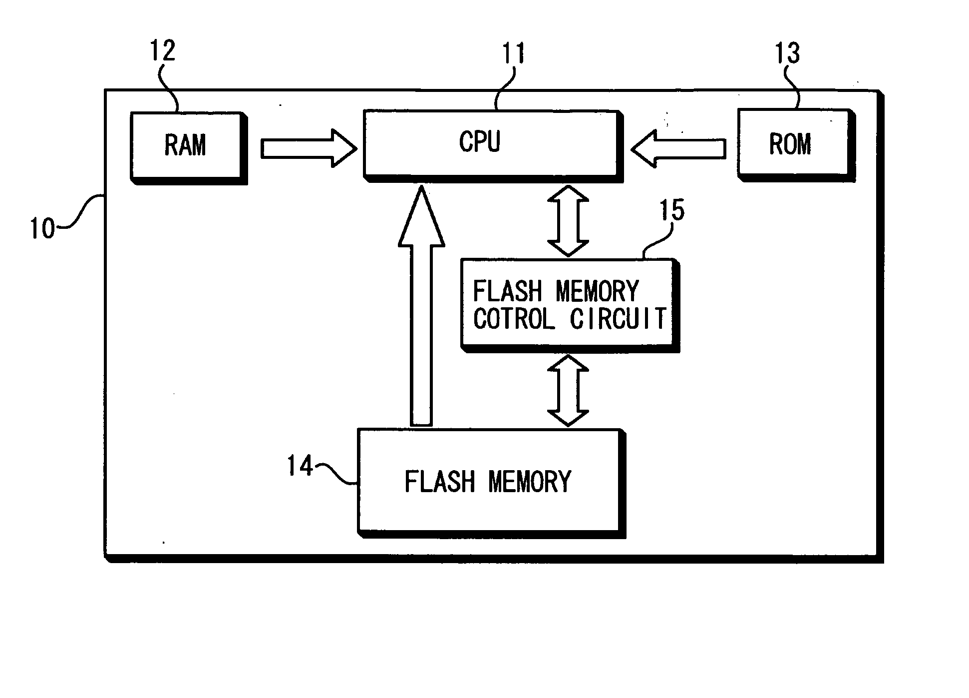
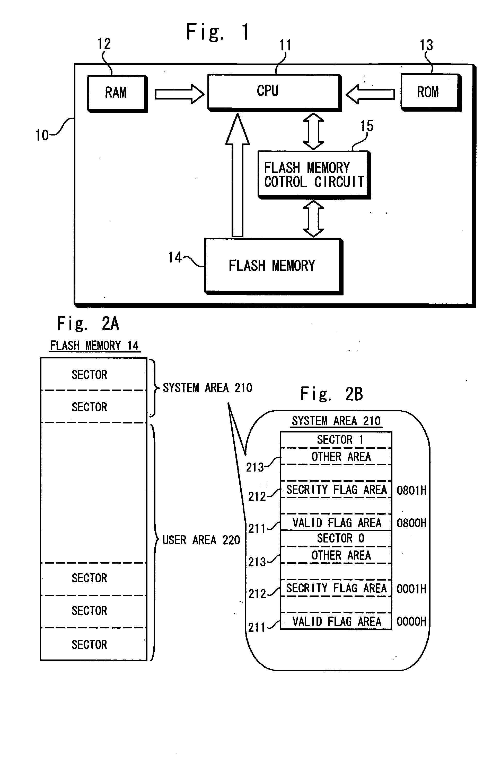
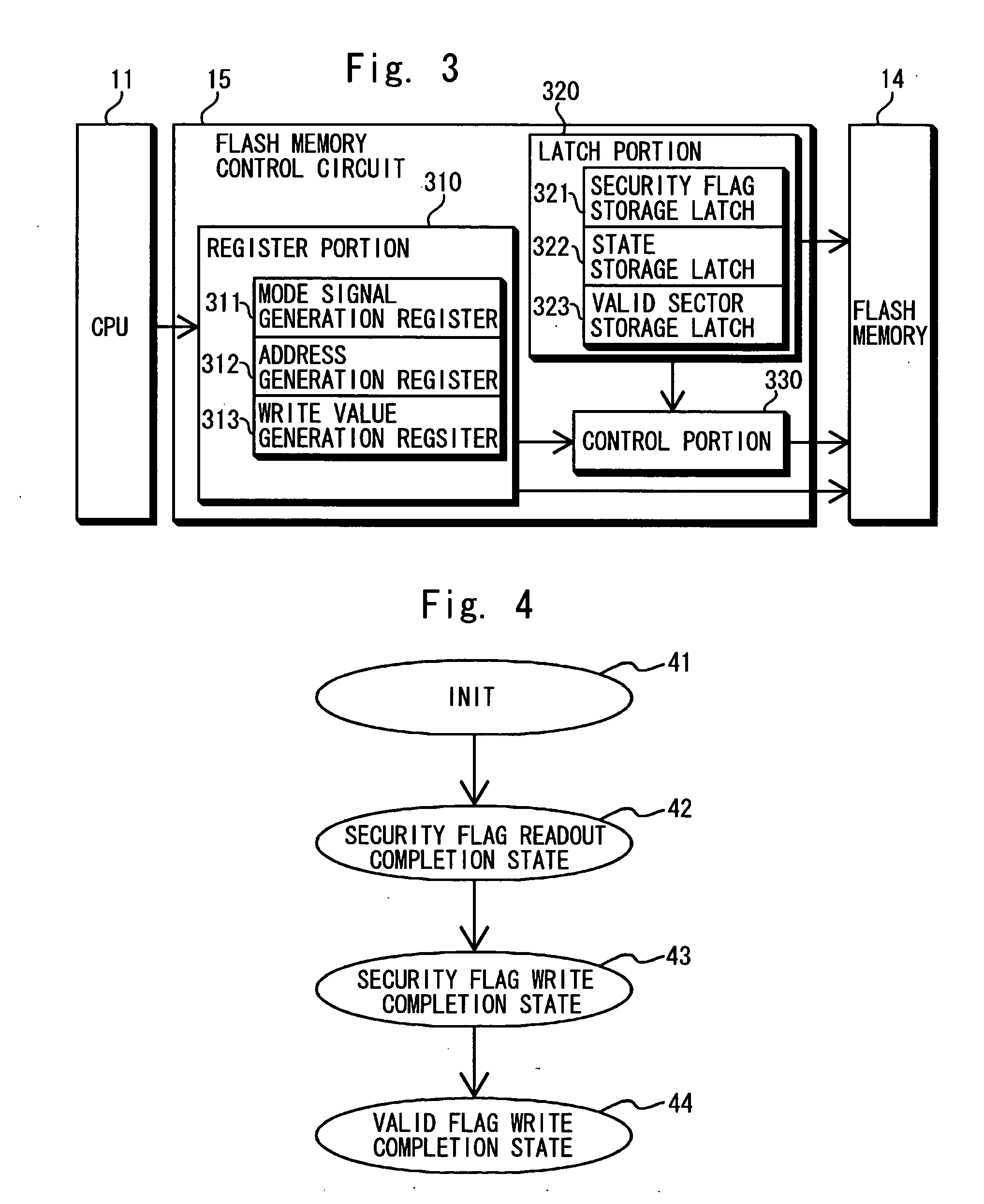
[0027] First, a structure of the microprocessor according to the first embodiment of the invention is explained with reference to FIG. 1. As shown in FIG. 1, the microprocessor 10 comprises a CPU 11, a RAM 12, a ROM 13, a flash memory 14 and a flash memory control circuit 15 (overwriting portion). The microprocessor 10 may additionally include input and output terminals. The CPU 11 is connected to the RAM 12, the ROM 13, the flash memory 14 and the flash memory control circuit 15 via buses or the like. The flash memory control circuit 15 is also connected to the flash memory 14.

[0028] The microprocessor 10 can be any microprocessor comprising the components shown in the figures, for example, an MPU (Micro Processing Unit), an MCU (Micro Controller Unit), or an ASIC (Application Specific Integrated Circuit). Also, the microprocessor 10 can be a one-chip microprocessor, or can be divided into a plurality of chips and connected therewith.

[0029] The microprocess...


PUM


Abstract

An electronic device comprises a first and a second nonvolatile memory areas respectively having a data area for storing data and an identifying information area for storing identifying information which indicates whether the data is valid or invalid, and an overwrite portion for overwriting data to the first and second memory areas, wherein the overwrite portion writes new data to the data area of the second memory area if old data is stored in the data area of the first memory area, and writes the identifying information to the identifying information area of the first or second memory area, the identifying information indicating that the data area of the second memory area is valid.

Description

BACKGROND OF THE INVENTION [0001] 1. Field of the Invention [0002] This invention relates to electronic devices, nonvolatile memories and methods of overwriting data in the nonvolatile memory which prevent damaged data caused by a power interruption. [0003] 2. Description of Related Art [0004] In nonvolatile memories, flash memories that are erasable and writable per sector are used for storing BIOS (Basic Input / Output System) for PCs (personal computers) and used in, for example, memory cards for digital cameras, home-use game machines and the like. [0005] Also, the microprocessors which incorporate the flash memory have been developed. This allows the overwriting of the program even if the microprocessor is mounted state on the circuit board. Further, this allows the self-programming that the program overwrites itself while the program in the microprocessor is running. [0006] For example, in the case where the system failure is caused by the power interruption that occurred when o...

Claims


Application Information

Patent Timeline
Patent Type & Authority Applications(United States)
IPC IPC(8): G11C8/02G06F12/16
CPCG06F11/1441
Inventor TOMINAGA, KENICHIRO
Owner NEC ELECTRONICS CORP
Why Eureka
Try Eureka