Organic light-emitting device, manufacturing method thereof, and electronic apparatus thereof

a light-emitting device and manufacturing method technology, applied in the direction of discharge tube/lamp details, discharge tube luminescnet screens, coatings, etc., can solve the problems of inability to achieve uniform light-emitting positions, the need for perfect multi-layer structures, and the inability to achieve the highest luminous efficiency

Inactive Publication Date: 2005-04-07
SEIKO EPSON CORP
View PDF3 Cites 48 Cited by
  • Summary
  • Abstract
  • Description
  • Claims
  • Application Information

AI Technical Summary

Problems solved by technology

OLEDs, described above in relation to the related art technology, are subject to some problems, which are discussed below.
Consequently, there is a problem in that a plurality of perfect multi layer structures are needed.
Therefore, a parallel arrangement of a layer interface with an electrode does not necessarily result in the highest luminous efficiency.
Then, for example, a problem in the case is that a higher voltage must be set to transport a greater number of holes to have light emission in the emissiv

Method used


Image

  • Organic light-emitting device, manufacturing method thereof, and electronic apparatus thereof
  • Organic light-emitting device, manufacturing method thereof, and electronic apparatus thereof
  • Organic light-emitting device, manufacturing method thereof, and electronic apparatus thereof

Examples


Embodiment Construction

[0068] The following sections describe an exemplary embodiment of the present invention.

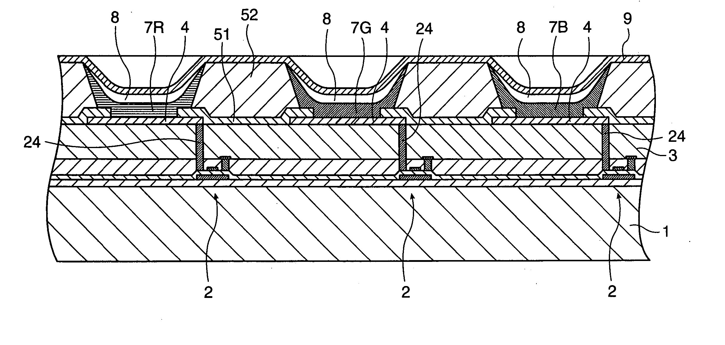
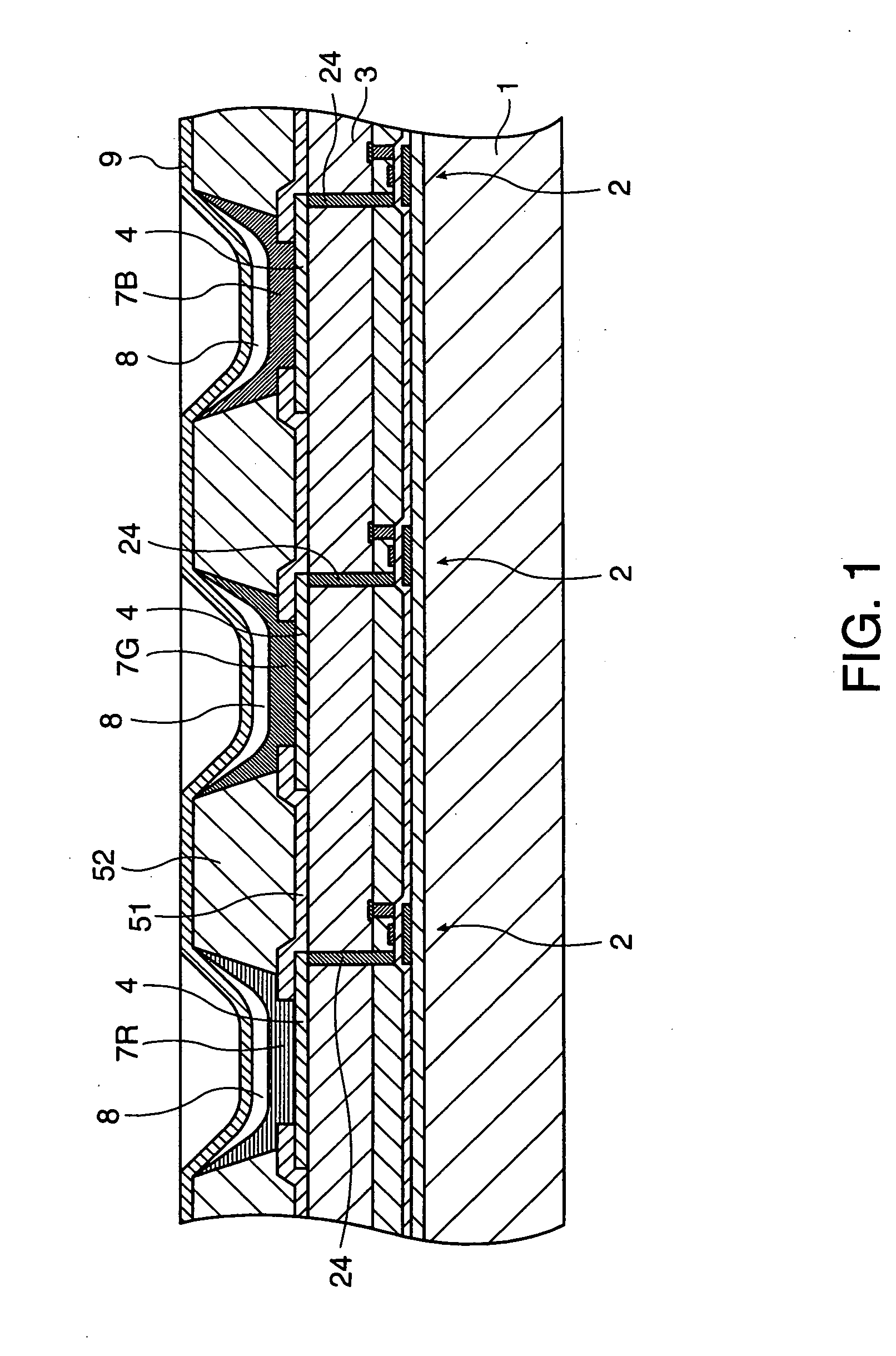
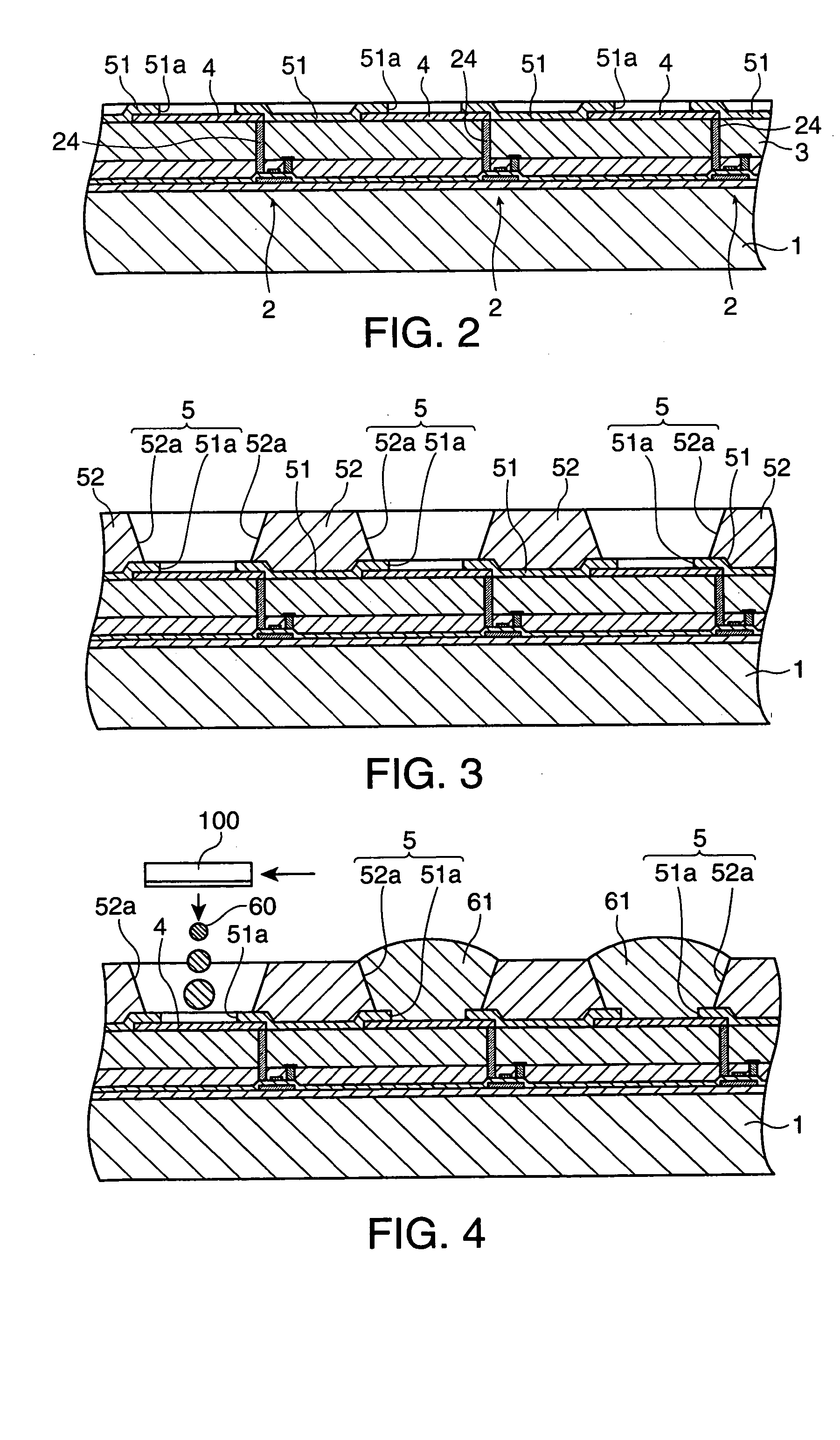
[0069] A method of manufacturing an OLED, which corresponds to an exemplary embodiment of the present invention, is described by referring to FIG. 1 to FIG. 10. In each drawing, a magnifying scale for each layer and each material component is different part by part to show each layer and each material component in recognizable size on the drawing.

[0070] The OLED to be manufactured here is a color OLED. As shown in FIG. 1; while a first organic EL element being equipped with a red emissive layer 7R, a second organic EL element being equipped with a green emissive layer 7G, and a third organic EL element being equipped with a blue emissive layer 7B; each organic EL element works as a pixel and eventually multiple pixels are placed on a substrate to have each pixel at a required position.

[0071] As shown in FIG. 2; on a glass substrate 1, a thin-film transistor 2 for each pixel is formed at first,...


PUM

PropertyMeasurementUnit
Percent by massaaaaaaaaaa
Solubility (mass)aaaaaaaaaa
Molecular weightaaaaaaaaaa

Abstract

An organic light-emitting device having a high efficiency in its luminous performance and a long product life, a method of manufacturing an organic light-emitting device, and an electronic apparatus are provided. The organic light-emitting device includes emissive functional layers formed between an anode and a cathode. A hole transport material and a emissive material are mixed in the emissive functional layers, while the hole transport material is provided with a host function, in which the emissive material works as a guest.

Description

BACKGROUND OF THE INVENTION [0001] 1. Field of Invention [0002] The present invention relates to an organic light-emitting device, a manufacturing method thereof, and an electronic apparatus thereof. [0003] 2. Description of Related Art [0004] Related art organic light-emitting devices (hereinafter “OLEDs”), including organic substances as a light-emitting display may replace liquid crystal displays. Related art methods to manufacture such OLEDs include a process to form thin films including small-molecular substances by a gas phase method, such as a depositing method, etc., as well as another process to form thin films including polymer substances by a liquid phase method. See Appl. Phys. Lett. 51(12), 21 Sep. 1987, p. 913 and Appl. Phys. Lett. 71(1), 7 Jul. 1997, p. 34. [0005] Further, as for coloring, in case of a small-molecular material, each of different emissive materials is deposited through a mask and formed on a desired pixel. In case of a polymer material, a coloring tech...

Claims


Application Information

Patent Timeline
IPC IPC(8): C09K11/06H01L51/00H01L51/30H01L51/50H01L51/56H05B33/10H05B33/18H05B33/26
CPCH01L27/3211H01L51/0034H01L51/0035H01L51/0036H01L51/56H01L51/0043H01L51/0059H01L51/5012H01L51/5221H01L51/0039H10K59/35H10K85/10H10K85/111H10K85/113H10K85/115H10K85/151H10K85/631H10K50/82H10K50/11H10K71/00C09K11/06H05B33/10H05B33/18
Inventor MORII, KATSUYUKITAKASHIMA, TAKESHIHOKARI, HIROFUMIMAKIURA, RIE
Owner SEIKO EPSON CORP
Why Eureka
Try Eureka