Novel integration of wire bond pad with Ni/Au metallization

a technology of ni/au metallization and wire bonding pads, which is applied in the direction of semiconductor devices, semiconductor/solid-state device details, electrical apparatus, etc., can solve the problems of poor wire bonding surface, damaged area bonding is not suitable for a low dielectric constant, and the availability of non-cyanide electroless gold chemistries, which are less stabl

Inactive Publication Date: 2005-04-07
GOOGLE LLC
View PDF17 Cites 48 Cited by
  • Summary
  • Abstract
  • Description
  • Claims
  • Application Information

AI Technical Summary

Benefits of technology

[0013] The wire bond pads that can be employed in the present invention include any conductive wire bond pad such as W, Al, Ta, Cu, and alloys thereof. Although the method of the present invention ca

Problems solved by technology

The amount of probing damage as a result of the “scrubbing” that is necessary to remove the native oxide on the Al wire bond pads causes a poor wire-bonding surface: Also, the force that is required for “scrubbing” Al bond pads and then consequently the bonding to the damaged area is not suitable for a lo

Method used


Image

  • Novel integration of wire bond pad with Ni/Au metallization
  • Novel integration of wire bond pad with Ni/Au metallization
  • Novel integration of wire bond pad with Ni/Au metallization

Examples


Embodiment Construction

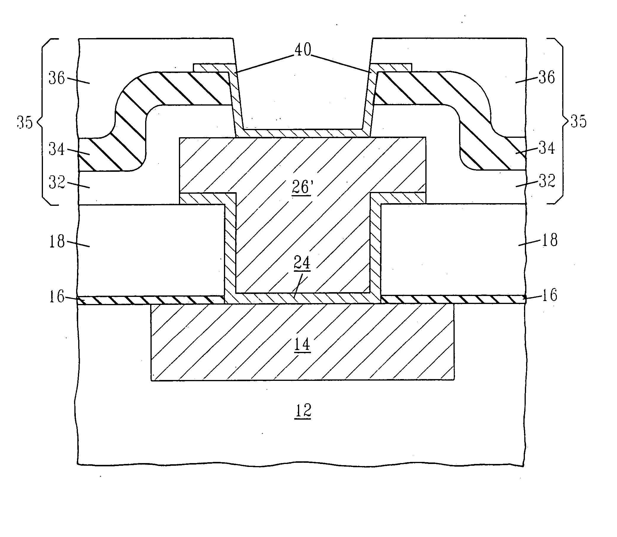
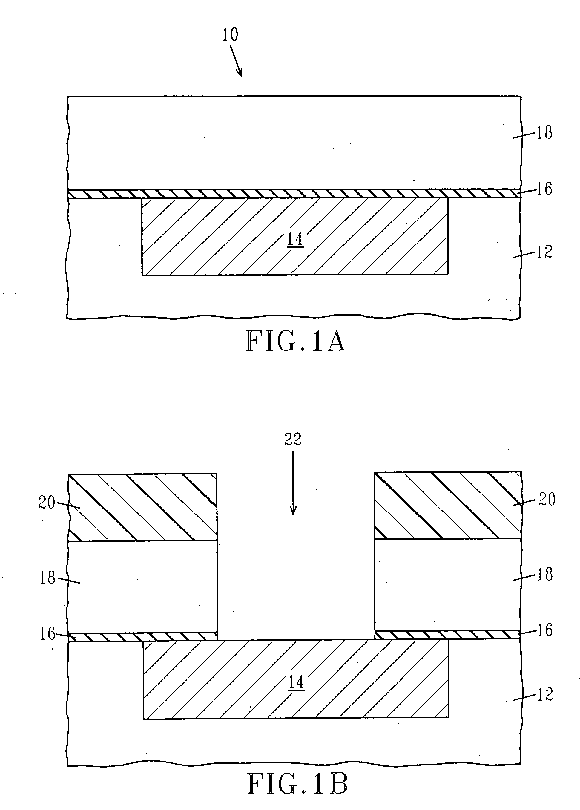
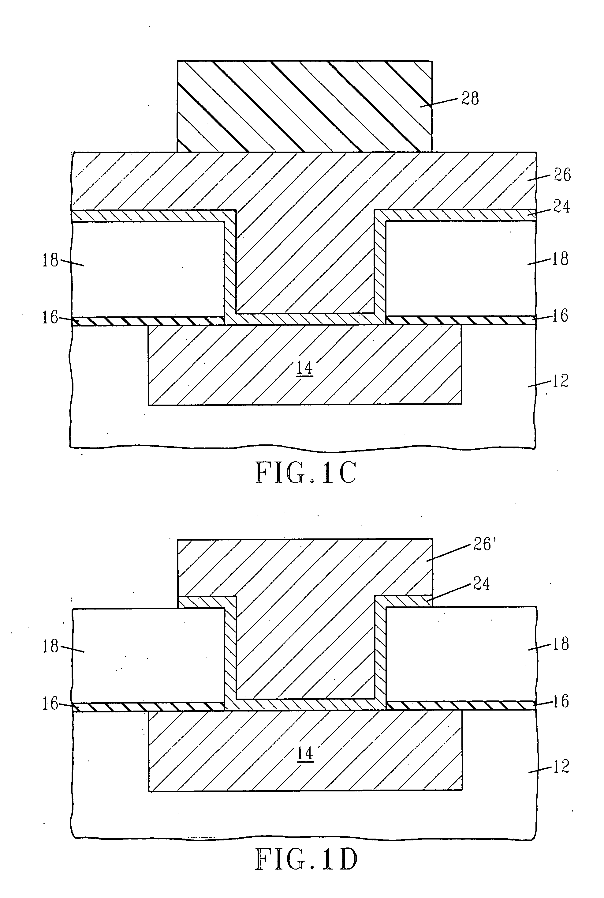
[0021] The present invention, which provides a method for protecting wire bond pads against chemical attack during formation of Ni / Au metallurgy, will now be described in greater detail by referring to the drawings that accompany the present application. In the accompanying drawings, like and / or corresponding elements are referred to by like reference numerals. Although the drawings and description that follow illustrate and discuss the presence of a single metal line, a single wire bond pad and a single Ni / Au pad metallization, the present invention is not limited thereto. Instead, the present invention can be used when any number of the foregoing elements is present in the structure. Moreover, the drawings of the present invention illustrate only the upper wiring level of an interconnect structure. Despite this illustration, the present invention contemplates using interconnect structure having a plurality of wiring levels, each stacked on top of each other.

[0022] Referring to FI...


PUM


Abstract

A method for sealing an exposed surface of a wire bond pad with a material that is capable of preventing a possible chemical attack during electroless deposition of Ni/Au pad metallurgy is provided. Specifically, the present invention provides a method whereby a TiN/Ti or TiN/Al cap is used as a protective coating covering exposed surfaces of a wire bond pad. The TiN/Ti or TiN/Al cap is not affected by alkaline chemistries used in forming the Ni/Au metallization, yet it provides a sufficient electrical pathway connecting-the bond pads to the Ni/Au pad metallization.

Description

BACKGROUND OF THE INVENTION [0001] The present invention relates to semiconductor device packaging, and more particularly to a process to seal the interfaces of wire bond pads, such as aluminum (Al) wire bond pads, thus preventing attack of the bond pads during the subsequent electroless plating of Ni / Au. BACKGROUND OF THE INVENTION [0002] In semiconductor manufacturing, a fabricated integrated circuit (IC) is usually assembled into a package to be utilized on a printed circuit board as part of a much larger circuit. In order for the leads of the board to make electrical contact with the bonding pads of the IC device, a metal bond, or wire, is formed to make a connection between the bond pad of an IC device and the lead extending to the package lead frame, or solder ball connection to a ceramic or polymeric chip. [0003] As the industry migrates to smaller and smaller size chips, finer pitch wire-bonding is required. The amount of probing damage as a result of the “scrubbing” that is...

Claims


Application Information

Patent Timeline
IPC IPC(8): H01L21/44H01L23/31H01L23/485H01L23/532
CPCH01L23/3192H01L23/53223H01L2924/00014H01L2224/45124H01L2924/01033H01L2924/01024H01L2924/01019H01L24/03H01L24/05H01L2224/04042H01L2224/0501H01L2224/05022H01L2224/05082H01L2224/05124H01L2224/05155H01L2224/05644H01L2924/01006H01L2924/01011H01L2924/01013H01L2924/01014H01L2924/01015H01L2924/01022H01L2924/01027H01L2924/01028H01L2924/01029H01L2924/0103H01L2924/01046H01L2924/0105H01L2924/01073H01L2924/01074H01L2924/01078H01L2924/01079H01L2924/01082H01L2924/014H01L2924/04941H01L2924/04953H01L2924/14H01L2924/00H01L2224/48H01L2224/02166H01L2224/48744H01L2924/12042
Inventor BURRELL, LLOYD G.DAVIS, CHARLES R.GOLDBLATT, RONALD D.LANDERS, WILLIAM F.MEHTA, SANJAY C.
Owner GOOGLE LLC
Why Eureka
Try Eureka