Data acknowledgment using impedance mismatching

a data acknowledgment and impedance mismatching technology, applied in the field of data acknowledgment using impedance mismatching, can solve the problems of circuit bulky circuit, complicated protocols for electronic components, and high cost, and achieve the effect of simple communication protocol

Inactive Publication Date: 2005-04-07
IBM CORP
View PDF9 Cites 0 Cited by
  • Summary
  • Abstract
  • Description
  • Claims
  • Application Information

AI Technical Summary

Benefits of technology

[0012] The present invention advantageously provides a simple communication protocol.

Problems solved by technology

Electronic components in a circuit typically require complicated protocols to communicate with each other.
Complicated protocols may require additional circuitry making the circuit bulky and costly.

Method used


Image

  • Data acknowledgment using impedance mismatching
  • Data acknowledgment using impedance mismatching
  • Data acknowledgment using impedance mismatching

Examples


Embodiment Construction

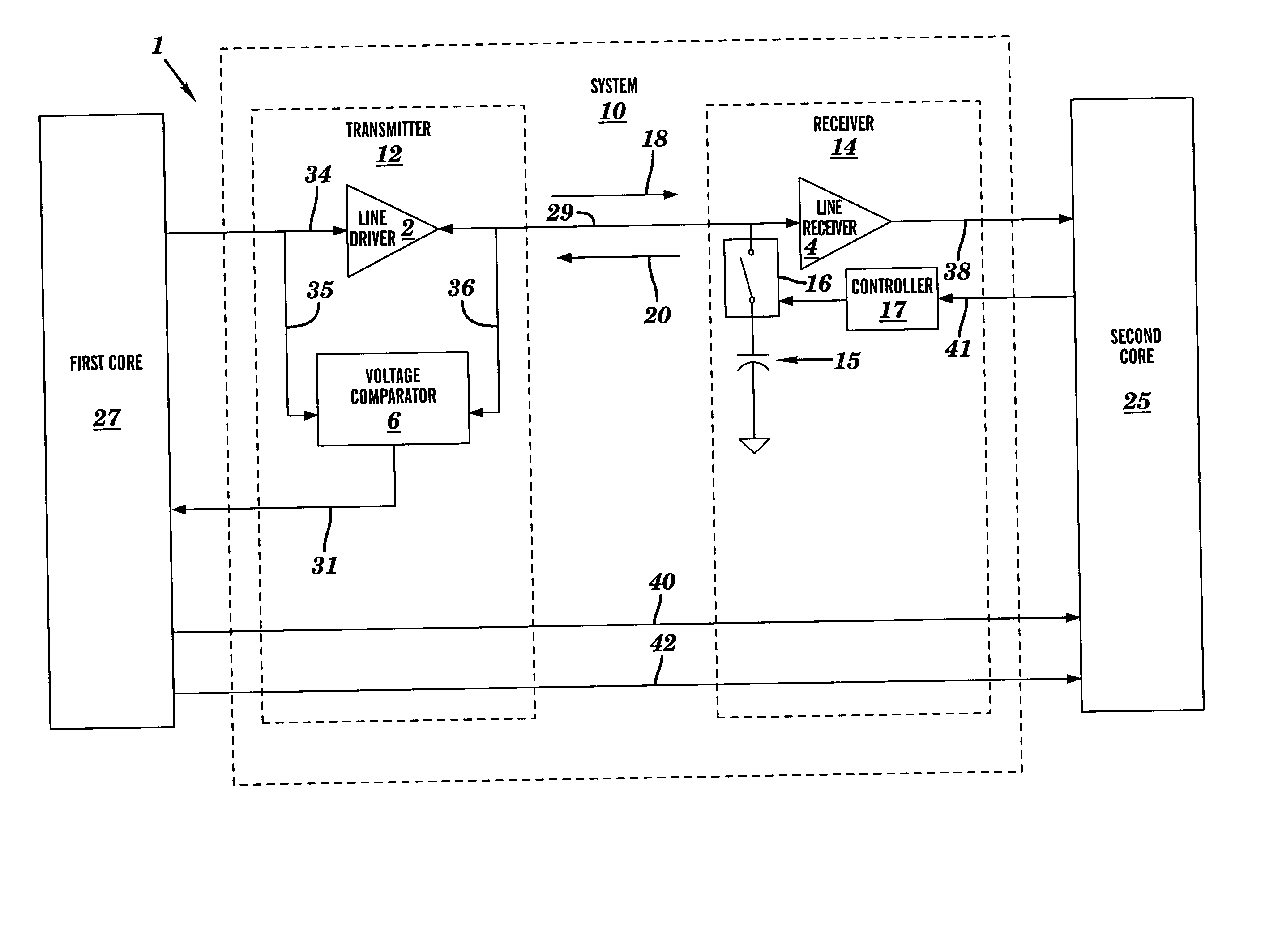
[0017]FIG. 1 is a block diagram view of a semiconductor device 1 comprising a system 10 to control data transfer between a first core 27 and a second core 25, in accordance with embodiments of the present invention. A core is defined herein as a functional area (i.e., adapted to perform a specified function) on the semiconductor device 1. The semiconductor device 1 may comprise a system on a chip (SOC). In FIG. 1, the semiconductor device 1 comprising the system 10, the first core 27, and the second core 25 are shown for illustrative purposes. The semiconductor device 1 may comprise a plurality of cores equivalent to each of the first core 27 and the second core 25. Additionally, the semiconductor device 1 may comprise a plurality of systems equivalent to the system 10. The system 10 is an interface for controlling the data flow between the first core 27 and the second core 25. The system 10 comprises a transmitter 12, a receiver 14, and a transmission line 29. The transmitter 12 co...


PUM


Abstract

A structure and associated method to control a flow of data on a semiconductor device. A transmitter, receiver and transmission line are formed within the semiconductor device. The transmitter, receiver, and transmission line are adapted to control data transfer between a first core and a second core within the semiconductor device. The transmitter is adapted to send a signal over the transmission line to the receiver adapted to receive the signal. The receiver is further adapted to create an impedance mismatch to indicate that the second core is unable to transfer the data. The transmitter is adapted to detect the impedance mismatch.

Description

BACKGROUND OF THE INVENTION [0001] 1. Technical Field [0002] The present invention relates to a structure and associated method to control data transfer between cores on a system on a chip. [0003] 2. Related Art [0004] Electronic components in a circuit typically require complicated protocols to communicate with each other. Complicated protocols may require additional circuitry making the circuit bulky and costly. Therefore there exists a need to create a simple communication protocol. SUMMARY OF THE INVENTION [0005] The present invention provides a semiconductor device, comprising: [0006] a transmitter, receiver, and transmission line formed within the semiconductor device, wherein the transmitter, receiver, and transmission line are adapted to control data transfer between a first core and a second core within the semiconductor device, wherein the transmitter is adapted to send a signal over the transmission line to the receiver adapted to receive the signal, wherein the receiver ...

Claims


Application Information

Patent Timeline
Patent Type & Authority Applications(United States)
IPC IPC(8): G06F12/00
CPCG06F13/4269
Inventor BOUDREAUX, MICHAEL J.COURCHESNE, ADAM J.NORMAN, JASON M.STYDUHAR, MARK S.VENTRONE, SEBASTIAN T.
Owner IBM CORP
Why Eureka
Try Eureka