Electrostatic capacitance detection device

a capacitance detection and electrostatic technology, applied in the field of electrostatic capacitance detection devices, can solve the problems of inability to operate stably, inability to withstand bending, so as to achieve superior electrostatic capacitance detection, reduce the expenditure of unnecessary energy and labor, and operate stably

Active Publication Date: 2005-04-14
138 EAST LCD ADVANCEMENTS LTD
View PDF8 Cites 26 Cited by
  • Summary
  • Abstract
  • Description
  • Claims
  • Application Information

AI Technical Summary

Benefits of technology

Taking the aforesaid situation into account, the invention is designed to provide a superior electrostatic capacitance detection device that operates stabl

Problems solved by technology

Hence, they are fragile and subject to breaking when too much finger pressure is applied when they are used as a fingerprint sensor.
In other words, the electrostatic capacitance detection devices of the prior art are not only expen

Method used


Image

  • Electrostatic capacitance detection device
  • Electrostatic capacitance detection device
  • Electrostatic capacitance detection device

Examples


Embodiment Construction

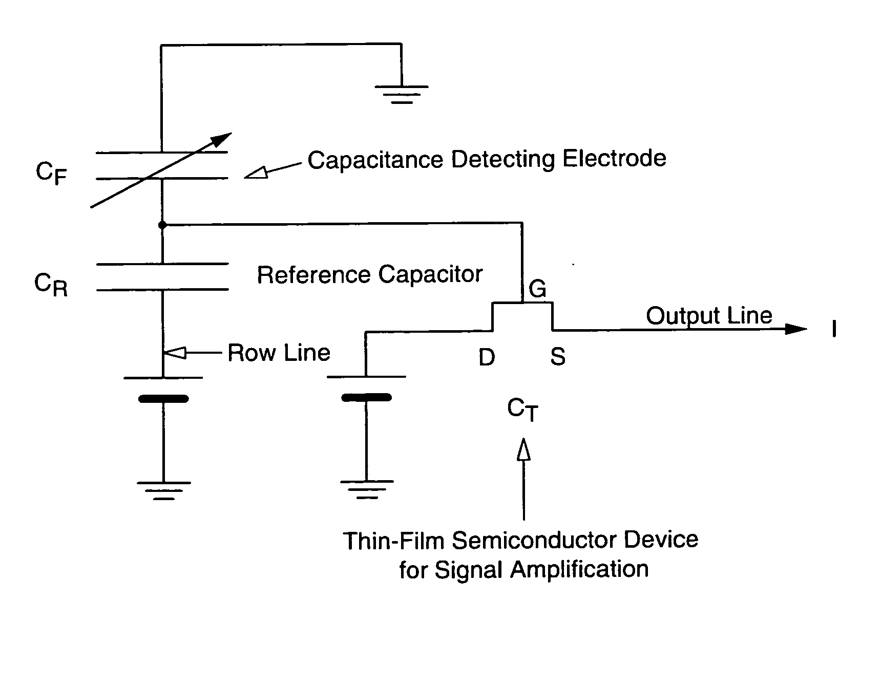
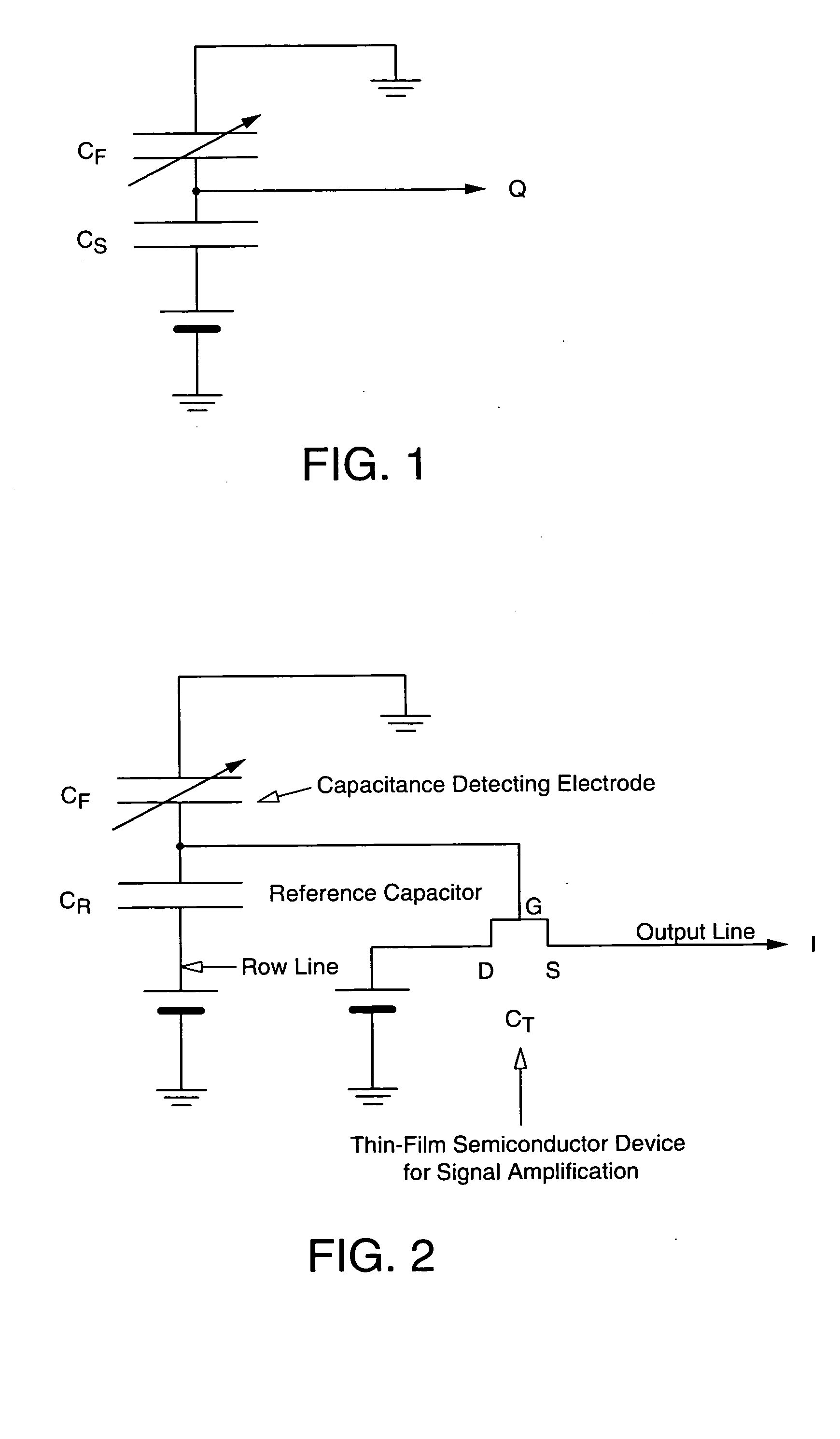
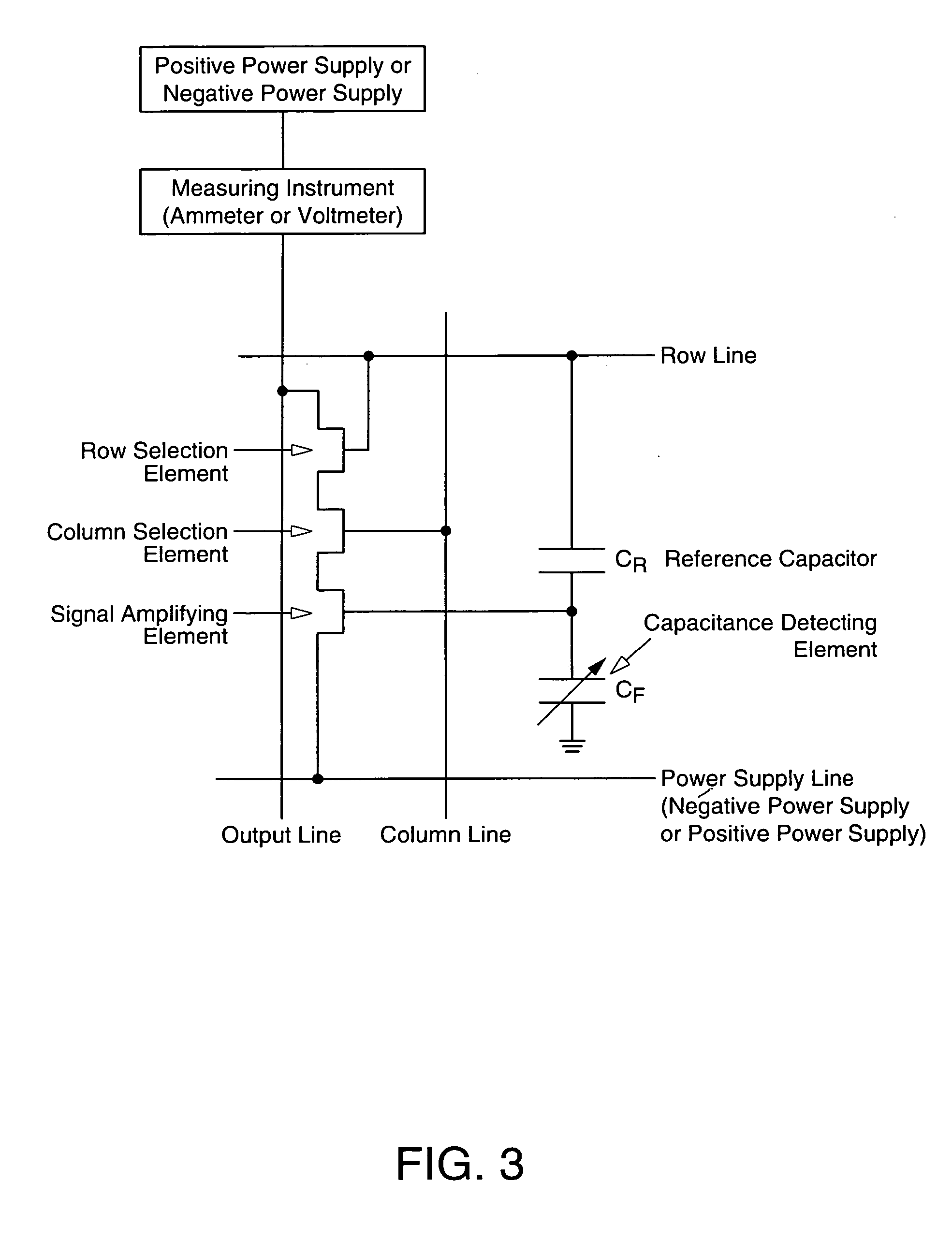
The invention can provide an electrostatic capacitance detection device that reads the surface contours of a target object by detecting electrostatic capacitance, which changes according to the distance from a target object. The electrostatic capacitance detection device is formed as an MIS thin-film semiconductor device comprising a metal-insulator-semiconductor layer. Since they are ordinarily fabricated on inexpensive glass substrates, thin-film semiconductor devices are generally known for their usefulness in inexpensively fabricating semiconductor integrated circuits that require a large area, specifically devices such as liquid crystal display devices. Therefore, fabricating thin-film semiconductor devices for use as an electrostatic capacitance detection device in a fingerprint sensor, for example, obviates the need to use an expensive substrate, such as a single-crystal silicon wafer, whose production consumes tremendous energy. Instead, the device can be fabricated inexpen...


PUM


Abstract

Aspects of the invention can provide an electrostatic capacitance detection device having M number of row lines and N number of column lines arranged in a matrix of M rows and N columns, and an electrostatic capacitance detection element formed at the intersection thereof. The electrostatic capacitance detection element can include a signal detection element, a signal amplifying element and a column selection element and a row selection element. The signal detection element can include a capacitance detecting electrode, a capacitance detecting dielectric layer, and a reference capacitor. One of a pair of electrodes in the reference capacitor is coupled to the row line. Accordingly, the invention can achieve a superior electrostatic capacitance detection device.

Description

BACKGROUND OF THE INVENTION 1. Field of Invention Aspects of the invention relate to an electrostatic capacitance detection device that reads the surface contours of a fingerprint or other target object having extremely small ridges and valleys, by detecting electrostatic capacitance, which changes according to the distance from the surface of the target object. 2. Description of Related Art As described in, for example, Japanese Unexamined Patent Publication Application No. Hei 11-118415, No. 2000-346608, No. 2001-56204, No. 2001-133213, and so forth, in related electrostatic capacitance detection devices that are used in fingerprint sensors and so forth, a sensor electrode and a dielectric layer deposited on the sensor electrode are formed on a single-crystal silicon wafer. The principle of operation of a related electrostatic capacitance detection device is shown in FIG. 1. One of a pair of electrodes in a capacitor is a sensor electrode, the other is grounded to a human. Fur...

Claims


Application Information

Patent Timeline
IPC IPC(8): A61B5/117G01B7/28G01R27/26G06K9/00G06T1/00H01L21/336H01L21/768H01L29/786
CPCG06K9/0002G06V40/1306
Inventor MIYASAKA, MITSUTOSHI
Owner 138 EAST LCD ADVANCEMENTS LTD
Why Eureka
Try Eureka