
Dual-ported read SRAM cell with improved soft error immunity

a dual-port read and soft error technology, applied in the field of sram cells, can solve the problems of soft error, soft error, alpha particles, etc., and achieve the effect of improving the soft error ra

Inactive Publication Date: 2005-04-14
HEWLETT PACKARD DEV CO LP
View PDF7 Cites 3 Cited by
  • Summary
  • Abstract
  • Description
  • Claims
  • Application Information

AI Technical Summary

Benefits of technology

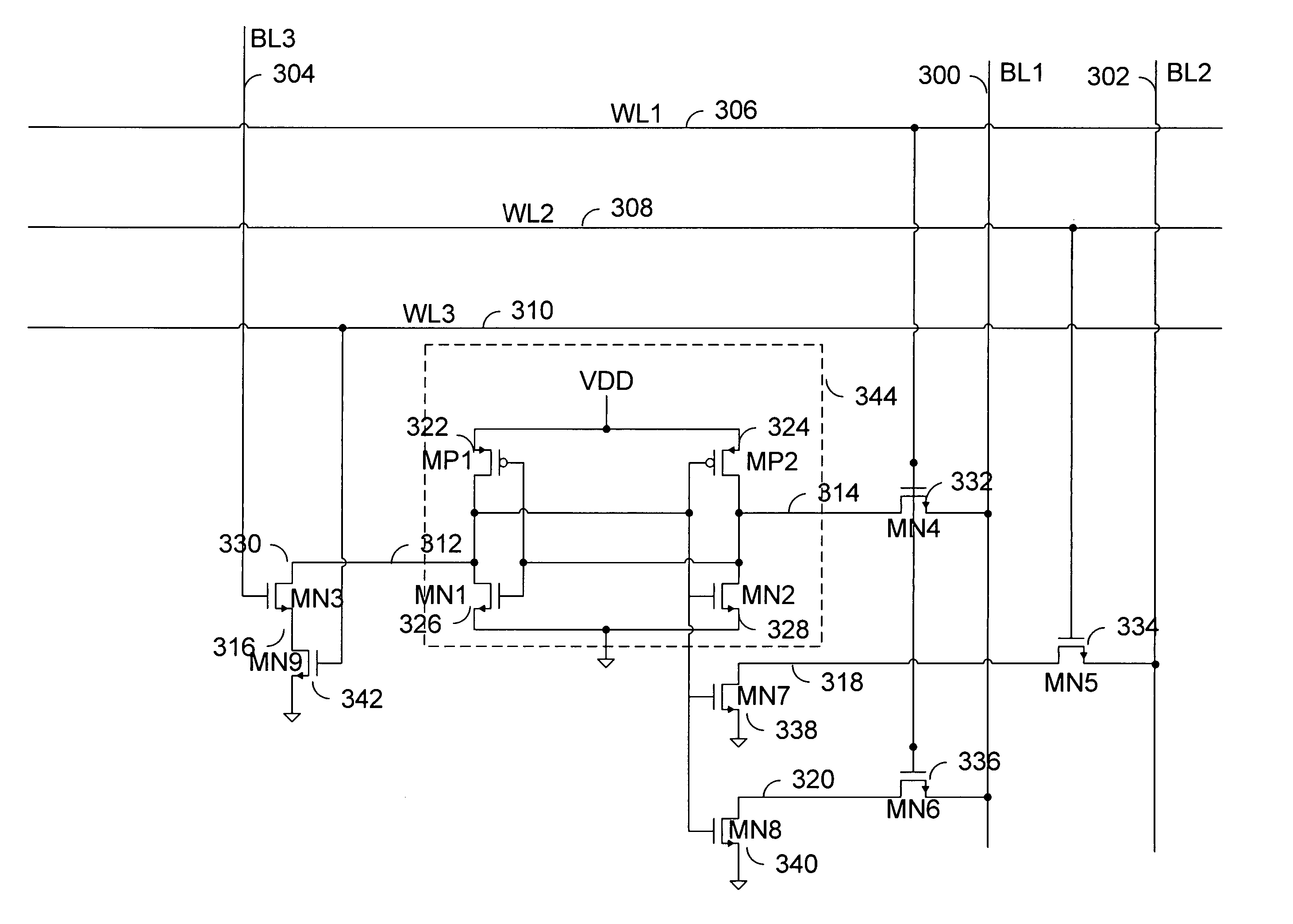
[0009] In a preferred embodiment, the invention provides a circuit and method for improving the soft error rate in a dual-port read SRAM cell. A write-only transfer device is connected to a cross-coupled latch, a first wordline, and a first bitline. A first read-only transfer device is connected to a second bitline, a second wordline, and a first pull-down device. A second read-only transfer device is connected to the first bitline, the first wordline, and a second pull-down device. A clear memory transfer device is connected to the cross-coupled latch, a third bitline, and a third pull-down device.
[0010] This configuration allows a reduction in the size of a dual-port SRAM cell with little or no reduction in the read access time of the cell. The reduction in size also reduces SER by reducing the cross-sectional, p / n junction area exposed to radiation.

Problems solved by technology

When a particle strikes a sensitive region of an SRAM (Static Random Access Memory) cell, the charge that accumulates could exceed the minimum charge that is needed to “flip” the value stored in the cell, resulting in a soft error.
A common source of soft errors are alpha particles, which may be emitted by trace amounts of radioactive isotopes present in packing materials of integrated circuits.
Neutrons can be particularly troublesome as they can penetrate most man-made construction (a neutron can easily pass through five feet of concrete).

Method used


Image

  • Dual-ported read SRAM cell with improved soft error immunity
  • Dual-ported read SRAM cell with improved soft error immunity
  • Dual-ported read SRAM cell with improved soft error immunity

Examples


Embodiment Construction

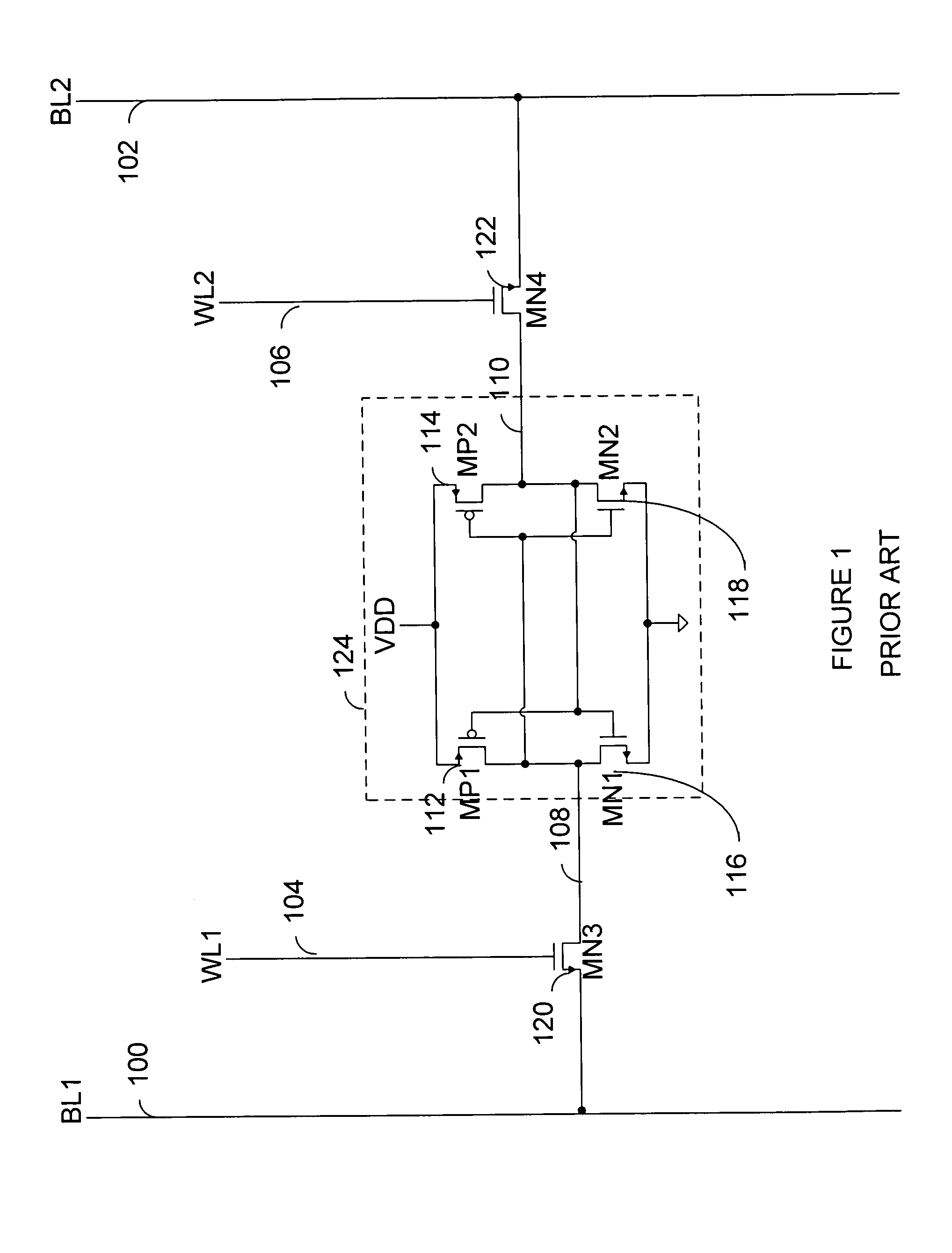
[0017]FIG. 1 is a schematic of a six transistor dual-port read SRAM cell. Bitline, BL1, 100 is connected to the source of NFET (N-type Field Effect Transistor), MN3, 120. Bitline, BL2, 102 is connected to the source of NFET, MN4, 122. Wordline, WL1, 104 is connected to the gate of NFET, MN3, 120. Wordline, WL2, 106 is connected to the gate of NFET, MN4, 122.

[0018] The drain, 108, of NFET, MN3, 120 is connected to the drain of PFET (P-type Field Effect Transistor), MP1, 112, the drain of NFET, MN1, 116, the gate of PFET, MP2, 114, and the gate of NFET, MN2, 118.

[0019] The drain, 110, of NFET, MN4, 122 is connected to the drain of PFET (P-type Field Effect Transistor), MP2, 114, the drain of NFET, MN2, 118, the gate of PFET, MP1, 112, and the gate of NFET, MN1, 116. A cross-coupled latch, 124, in this example, includes PFET, MP1, 112, MP2, 114, MN1, 116, MN2, 118, and the connections made to them.

[0020] Data may be read from the SRAM cell shown in FIG. 1 in two ways. A first way is...


PUM


Abstract

In a preferred embodiment, the invention provides a circuit and method for improving the soft error rate in a dual-port read SRAM cell. A write-only transfer device is connected to a cross-coupled latch, a first wordline, and a first bitline. A first read-only transfer device is connected to a second bitline, a second wordline, and a first pull-down device. A second read-only transfer device is connected to the first bitline, the first wordline, and a second pull-down device. A clear memory transfer device is connected to the cross-coupled latch, a third bitline, and a third pull-down device. This configuration allows a reduction in the size of a dual-port SRAM cell with little or no reduction in the read access time of the cell. The reduction in size also reduces SER by reducing the cross-sectional, p / n junction area exposed to radiation.

Description

FIELD OF THE INVENTION [0001] This invention relates generally to SRAM cells. More particularly, this invention relates to improving soft error immunity on dual-ported read SRAM cells. BACKGROUND OF THE INVENTION [0002] High-energy neutrons lose energy in materials mainly through collisions with silicon nuclei that lead to a chain of secondary reactions. These reactions deposit a dense track of electron-hole pairs as they pass through a p-n junction. Some of the deposited charge will recombine, and some will be collected at the junction contacts. When a particle strikes a sensitive region of an SRAM (Static Random Access Memory) cell, the charge that accumulates could exceed the minimum charge that is needed to “flip” the value stored in the cell, resulting in a soft error. [0003] The smallest charge that results in a soft error is called the critical charge of the SRAM cell. The rate at which soft errors occur (SER) is typically expressed in terms of failures in time (FIT). [0004] ...

Claims


Application Information

Patent Timeline
Patent Type & Authority Applications(United States)
IPC IPC(8): G11C8/16G11C11/41G11C11/412
CPCG11C11/4125G11C8/16
Inventor RIEDLINGER, REID JAMESYELTON, BRANDONAFFLECK, STEVEN R.
Owner HEWLETT PACKARD DEV CO LP
Learn More