Probe apparatus

Inactive Publication Date: 2005-04-21
TOKYO SEIMITSU
View PDF5 Cites 37 Cited by
  • Summary
  • Abstract
  • Description
  • Claims
  • Application Information

AI Technical Summary

Benefits of technology

[0016] A probe apparatus according to the invention includes displacement detection means for detecting displacement of the position of a probe card, disposed on a surface of the probe card and control means for moving a stage supporting thereon the wafer in a Z axis direction in accordance with a signal from the displacement detection means, wherein the stage is moved and corrected in the Z axis direction in accordance with detection of displacement of the position of the probe card from the wafer by the displacement detection means so that a contact condition between t

Problems solved by technology

However, because the probe card of the prior art is fixed at its periphery by a card retaining member, the probe card undergoes deformation in such a manner as to warp, as a whole, when thermal expansion occurs.
Therefore, the contact position between the probing needle of the probe card and the electrode pad of the semiconductor pad deviates from the position of positioning before the measurement and their contact becomes insufficient.
In consequence, the test measure cannot be made with high accuracy or the electrode pad is damaged due to an excessively strong contact.
However, the change of the material of the card holder to the material that is not easily affected by the influences of heat involves the problem that the material cost and the production cost increase.
Therefore, as the probing needle is measured while being spaced apart from the heat source (stage), the measurement is conducted at a lower temperature than the temperature of the contact condition between the probing needle and the electrode pad, so that an accurate measurement result cannot be obtained.
Because the distal end position of the probing needle must be re-measured

Method used


Image

  • Probe apparatus
  • Probe apparatus
  • Probe apparatus

Examples


Embodiment Construction

[0023] A probe apparatus according to an embodiment of the invention will be hereinafter explained with reference to the drawings.

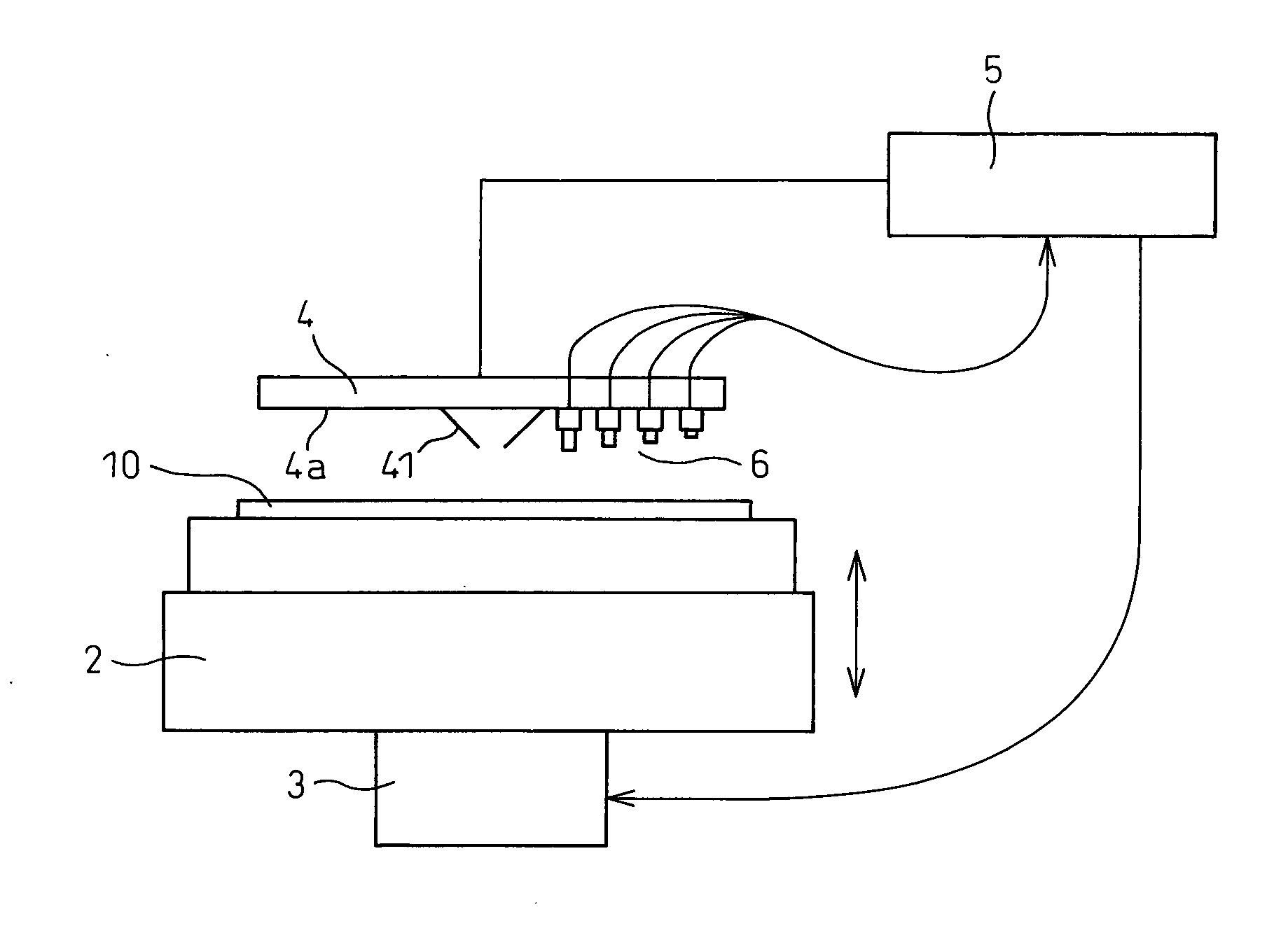
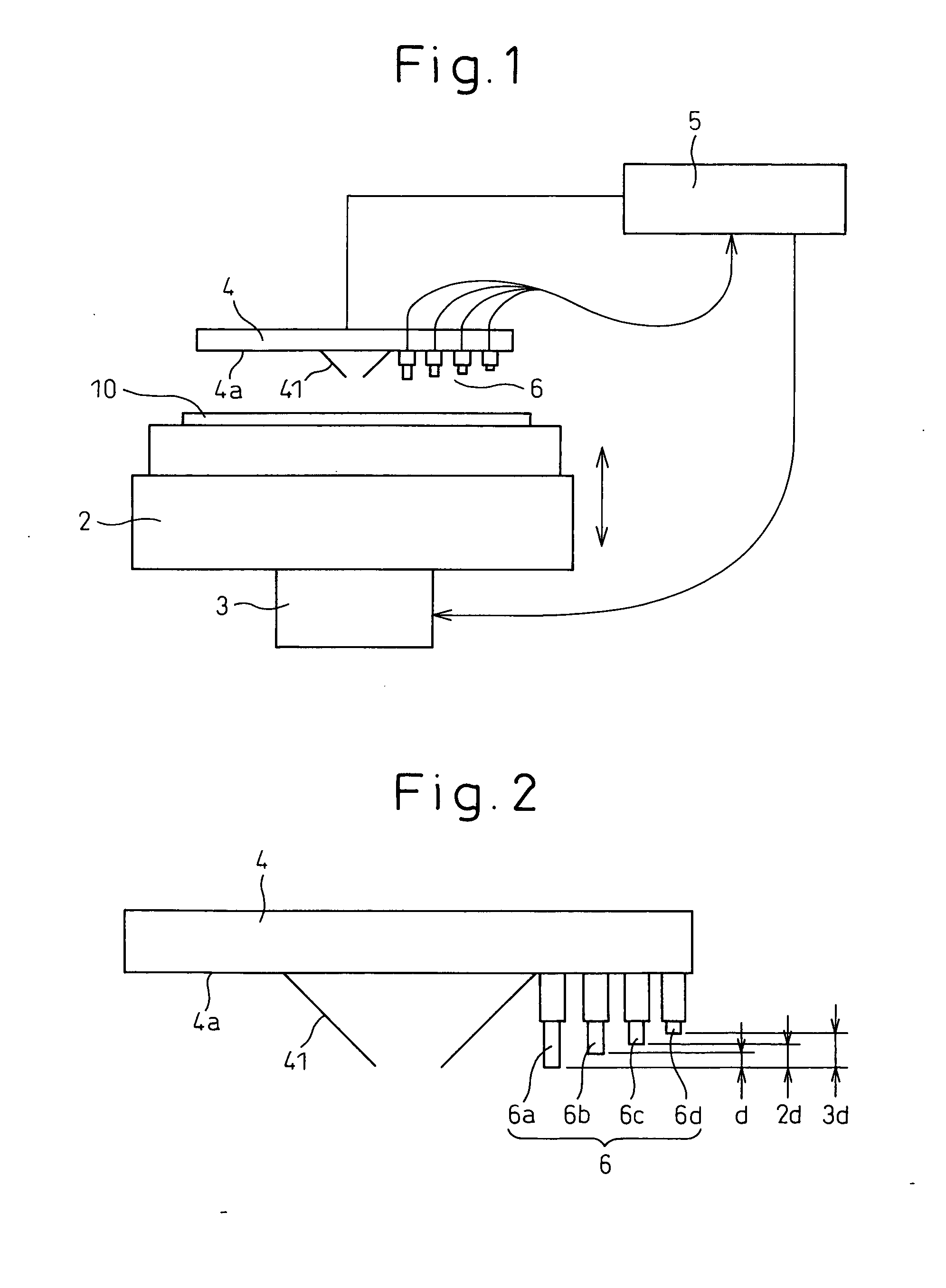
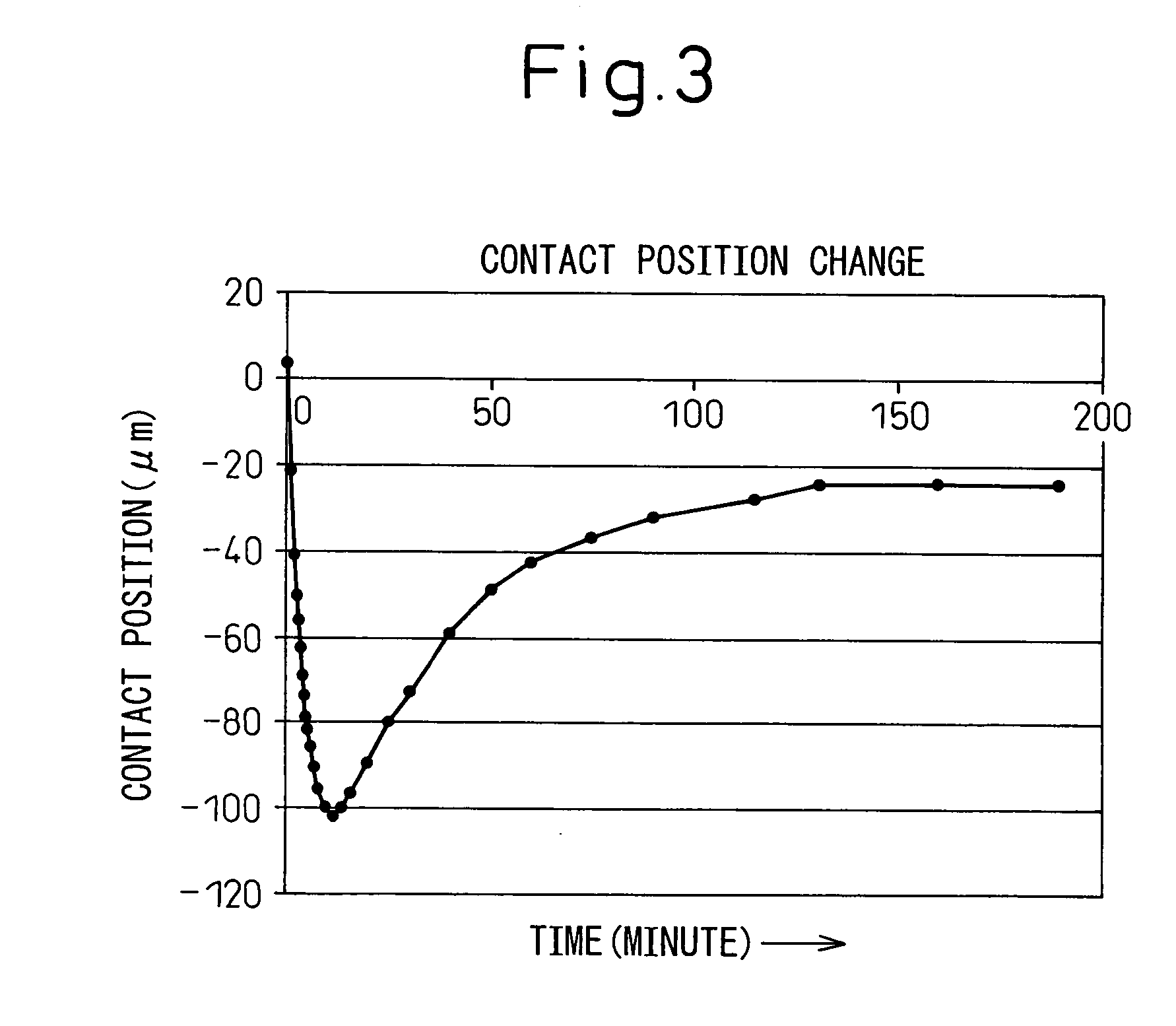
[0024]FIG. 1 schematically shows an overall construction of the probe apparatus according to the embodiment of the invention. The probe apparatus 1 includes a stage 2, a stage driving mechanism 3, a probe card 4 having probing needles 41, a tester 5 and displacement detection means 6.

[0025] A stage 2 having a chuck mechanism for placing and holding a wafer 10 is so constituted by the stage driving mechanism 3 controlled by the tester 5 and a control portion (not shown) as to be capable of moving in X, Y and Z directions and a 0 rotation direction the center of which lies in a Z axis and can thus three-dimensionally move the wafer 10.

[0026] A large number, that is, hundreds or thousands, of bump-like electrode pads (not shown in the drawing) are formed on the surface of a large number of semiconductor devices formed on the wafer 10. Probing needles 41 c...


PUM


Abstract

A probe apparatus 1 includes displacement detection means 6 disposed on a surface 4a of a probe card 4 from which probing needles 41 of the probe card 4 protrude, and control means 5 for receiving a signal of a positional change of the probe card 4 from the displacement detection means or a positional change on the stage side, or signals of positional changes of both of them and moving a stage 2 in a Z axis direction. The displacement detection means detects on the real time basis the positional change of the probe card due to influences of heat, etc, moves the stage to correct the positional change and keeps the contact condition between probing needles of the probe card and electrode pads of a wafer 10 always constant.

Description

CROSS REFERENCE TO RELATED APPLICATION [0001] This application claims the priority of Japanese Patent Application Number 2003-297630, filed on Aug. 21, 2003. BACKGROUND OF THE INVENTION [0002] 1. Field of the Invention [0003] This invention relates to a probe apparatus for inspecting electric characteristics of a plurality of semiconductor devices formed on a wafer. More particularly, the invention relates to a probe apparatus that can correct, on a real time basis, a positional change of a probe card, a positional change of a stage on which the wafer is put or the positional changes of both probe card and stage (contact position change) due to the influence of heat in case of inspecting in an environment such as high or low temperatures. [0004] 2. Description of the Related Art [0005] A large number of semiconductor devices having the same electric element circuit formed therein are formed on a surface of a wafer. To inspect the electric characteristics of each electric element cir...

Claims


Application Information

Patent Timeline
IPC IPC(8): G01R31/26G01R1/06G01R1/073G01R31/28H01L21/66
CPCG01R31/2891G01R31/2887
Inventor NIHEI, MAKOTOUEDA, YUTAKA
Owner TOKYO SEIMITSU
Why Eureka
Try Eureka